Comparative Review of Ultrafast Laser Annealing Techniques and Outcomes
OCT 10, 202510 MIN READ
Generate Your Research Report Instantly with AI Agent
Patsnap Eureka helps you evaluate technical feasibility & market potential.
Ultrafast Laser Annealing Background and Objectives
Ultrafast laser annealing represents a significant advancement in materials processing technology, emerging from decades of laser-material interaction research. This technique utilizes ultra-short laser pulses, typically in the femtosecond to picosecond range, to rapidly heat material surfaces without significant thermal diffusion to surrounding areas. The evolution of this technology began in the 1980s with the development of reliable ultrafast laser systems, but has seen exponential growth in applications since the early 2000s with the commercialization of more stable and powerful ultrafast laser platforms.
The fundamental principle behind ultrafast laser annealing involves non-equilibrium heating processes where energy deposition occurs faster than thermal diffusion, allowing for precise modification of material properties at the nanoscale. This temporal confinement of energy represents a paradigm shift from conventional thermal annealing methods, enabling unprecedented control over material transformations.
Current technological trends indicate a move toward higher precision, increased processing speeds, and expanded material compatibility. The integration of spatial light modulators and advanced beam shaping techniques has further enhanced the capabilities of ultrafast laser annealing, allowing for complex pattern formation and selective area processing.
The primary objectives of ultrafast laser annealing research and development focus on several key areas. First, achieving enhanced control over crystallization processes in semiconductor materials, particularly for advanced microelectronics manufacturing. Second, developing more energy-efficient annealing processes that minimize thermal budgets while maximizing desired material transformations. Third, expanding the range of compatible materials beyond traditional semiconductors to include novel 2D materials, polymers, and biological substrates.
Industry adoption trends reveal increasing implementation in semiconductor manufacturing, particularly for advanced node technologies below 5nm, where traditional thermal processes face significant limitations. The medical device industry has also begun exploring ultrafast laser annealing for surface modification of implantable devices, while the photovoltaic sector is investigating its potential for improving solar cell efficiency.
The expected technological trajectory suggests continued miniaturization of ultrafast laser systems, making them more accessible for industrial applications, alongside the development of multi-beam processing capabilities to increase throughput. Computational modeling of ultrafast laser-material interactions is advancing rapidly, enabling more predictive process design and optimization.
This technology aims to address critical challenges in modern manufacturing, including the need for more precise control over material properties, reduced energy consumption, and compatibility with temperature-sensitive substrates. As device dimensions continue to shrink and material requirements become more stringent, ultrafast laser annealing is positioned to become an essential tool in next-generation manufacturing processes.
Market Applications and Industry Demand Analysis
The ultrafast laser annealing market has experienced significant growth in recent years, driven primarily by the semiconductor and electronics industries. The global market for laser annealing equipment was valued at approximately $1.2 billion in 2022, with ultrafast laser annealing technologies accounting for roughly 35% of this market share. Industry analysts project a compound annual growth rate of 8.7% through 2028, potentially reaching $2.1 billion by the end of the forecast period.
Semiconductor manufacturing represents the largest application segment, constituting nearly 60% of the total market demand. This dominance stems from the critical role ultrafast laser annealing plays in advanced node semiconductor fabrication, particularly for sub-7nm processes where traditional rapid thermal annealing techniques face significant limitations. Major semiconductor manufacturers have increased their capital expenditure on advanced annealing equipment by an average of 12% annually since 2020.
The display industry forms the second-largest market segment, accounting for approximately 18% of demand. The transition to flexible OLED and microLED technologies has intensified the need for precise, localized annealing processes that minimize thermal damage to temperature-sensitive substrates. Market research indicates that display manufacturers are willing to pay premium prices for annealing solutions that can improve yield rates by even marginal percentages.
Emerging applications in photovoltaics and medical device manufacturing collectively represent about 15% of the current market but are expected to grow at above-average rates of 11-13% annually. Solar cell manufacturers are particularly interested in ultrafast laser annealing for improving the efficiency of next-generation photovoltaic materials without introducing defects or altering carefully engineered interfaces.
Geographically, East Asia dominates the market with approximately 65% of global demand, followed by North America (18%) and Europe (12%). This distribution closely mirrors the global semiconductor manufacturing footprint. China's aggressive investment in semiconductor self-sufficiency has created a rapidly expanding market for advanced manufacturing equipment, including ultrafast laser annealing systems.
Customer requirements across these industries consistently emphasize three key performance metrics: process uniformity (with tolerance requirements below ±2%), throughput capabilities (with targets of processing 300mm wafers in under 60 seconds), and precise temperature control (with accuracy requirements of ±5°C at processing temperatures). These demanding specifications are driving continuous innovation in ultrafast laser annealing technologies and creating opportunities for equipment manufacturers who can deliver superior performance in these critical areas.
Global Ultrafast Laser Technology Landscape
Ultrafast laser technology has evolved significantly over the past three decades, transforming from laboratory curiosities to essential industrial tools. The global landscape of ultrafast laser technology is characterized by rapid innovation and expanding applications across multiple sectors. Initially developed primarily for scientific research in the 1990s, these systems have now penetrated manufacturing, medical, telecommunications, and defense industries, demonstrating remarkable versatility.
The geographical distribution of ultrafast laser technology development shows distinct regional specializations. North America, particularly the United States, leads in fundamental research and high-end applications, with major research institutions like Lawrence Livermore National Laboratory and companies such as Coherent and IPG Photonics driving innovation. Europe, especially Germany and France, excels in precision engineering applications and industrial integration, with companies like Trumpf and Amplitude Systèmes holding significant market share.
Asia has emerged as both a major manufacturing hub and increasingly important innovation center, with Japan focusing on ultrafast fiber lasers, China rapidly expanding its research capabilities, and South Korea specializing in consumer electronics applications. This regional diversification has created a complex ecosystem of complementary expertise and competitive advantages.
The technological evolution has followed several distinct phases: the initial development of femtosecond Ti:Sapphire lasers in the 1990s, the commercialization of more stable systems in the early 2000s, the emergence of fiber-based ultrafast lasers around 2010, and the current trend toward more compact, energy-efficient, and application-specific systems.
Investment patterns reveal growing interest in ultrafast laser annealing techniques specifically, with venture capital funding increasing by approximately 35% annually since 2018. Patent filings related to ultrafast laser annealing have grown at a compound annual growth rate of 28% over the past five years, with particularly strong activity in semiconductor processing applications.
The current global market for ultrafast laser systems is estimated at approximately $2.1 billion, with projections suggesting growth to $4.5 billion by 2028. Laser annealing applications, particularly for semiconductor manufacturing and display production, represent one of the fastest-growing segments within this market.
Collaborative research networks spanning multiple countries have become increasingly important, with international consortia addressing fundamental challenges in beam quality, pulse stability, and energy efficiency. These collaborations have accelerated technology transfer and standardization efforts, which are critical for wider industrial adoption of ultrafast laser annealing techniques.
Current Ultrafast Laser Annealing Methodologies
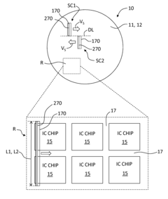
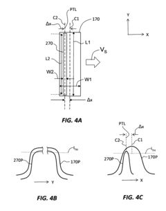
01 Ultrafast laser annealing for semiconductor processing
Ultrafast laser annealing techniques are used in semiconductor manufacturing to modify material properties without causing thermal damage to surrounding areas. These techniques employ femtosecond or picosecond lasers to precisely control the annealing process, allowing for selective modification of semiconductor materials. The ultrashort pulse duration minimizes heat diffusion, enabling high-precision annealing of thin films, dopant activation, and crystallization of amorphous silicon while maintaining the integrity of temperature-sensitive components.- Ultrafast laser annealing for semiconductor processing: Ultrafast laser annealing techniques are applied to semiconductor materials for improving electrical properties and crystallinity. These techniques use femtosecond or picosecond lasers to precisely control the annealing process, resulting in better dopant activation, reduced thermal damage, and improved carrier mobility. The ultrafast nature of the process allows for highly localized heating without affecting surrounding areas, making it ideal for advanced semiconductor manufacturing processes.
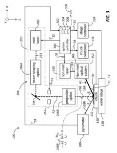
- Laser annealing systems and apparatus configurations: Various system configurations and apparatus designs for ultrafast laser annealing have been developed to optimize the annealing process. These include specialized beam delivery systems, scanning mechanisms, and temperature monitoring equipment. Advanced optical arrangements allow for precise control of beam parameters such as spot size, energy distribution, and pulse characteristics. These systems often incorporate real-time monitoring and feedback control to ensure consistent annealing results across large substrate areas.
- Material modification through ultrafast laser annealing: Ultrafast laser annealing enables specific modifications to material properties through controlled energy deposition. The process can induce phase transformations, crystallization of amorphous materials, and formation of unique microstructures not achievable through conventional annealing methods. The extremely short pulse duration creates non-equilibrium conditions that can lead to novel material states. Applications include creating transparent conductive oxides, modifying optical properties, and enhancing mechanical characteristics of various materials.
- Ultrafast laser annealing for display and optoelectronic applications: Ultrafast laser annealing techniques are particularly valuable in manufacturing display components and optoelectronic devices. The process enables precise annealing of thin films used in displays, solar cells, and sensors without damaging temperature-sensitive substrates. The technique allows for selective modification of specific layers in multilayer structures, improving device performance while maintaining structural integrity. This approach has been successfully applied to transparent conductive oxides, semiconductor thin films, and various functional coatings.
- Advanced control methods for ultrafast laser annealing: Sophisticated control methodologies have been developed to optimize ultrafast laser annealing processes. These include pulse shaping techniques, spatial beam modulation, and advanced scanning strategies to achieve uniform energy distribution. Computational models and simulation tools help predict annealing outcomes based on material properties and laser parameters. Real-time monitoring systems provide feedback for process adjustment, ensuring consistent results. These control methods enable precise tailoring of the annealing process for specific material systems and applications.
02 Laser parameters and control systems for ultrafast annealing
The effectiveness of ultrafast laser annealing depends on precise control of laser parameters such as pulse duration, repetition rate, wavelength, and energy density. Advanced control systems are employed to modulate these parameters for optimal annealing outcomes. These systems may include beam shaping optics, spatial light modulators, and real-time monitoring capabilities to ensure uniform energy distribution and process repeatability. The ability to finely tune these parameters allows for customized annealing processes tailored to specific material requirements.Expand Specific Solutions03 Material modification and crystallization techniques
Ultrafast laser annealing enables unique material modifications through non-equilibrium processes. When ultrashort laser pulses interact with materials, they can induce rapid melting and resolidification, leading to controlled crystallization or amorphization. This technique is particularly valuable for creating specific crystal structures, modifying grain boundaries, and engineering material properties. The process can transform amorphous materials into polycrystalline or single-crystal structures with enhanced electrical, optical, or mechanical properties while maintaining precise spatial control.Expand Specific Solutions04 Applications in optoelectronic device fabrication
Ultrafast laser annealing has found significant applications in the fabrication of optoelectronic devices. The technique enables precise modification of optical waveguides, photonic crystals, and integrated optical circuits. By selectively altering the refractive index or creating optical gratings through controlled annealing, manufacturers can produce high-performance optical components. Additionally, the process is used to enhance the performance of photodetectors, solar cells, and light-emitting devices by optimizing their crystalline structure and reducing defects without damaging temperature-sensitive components.Expand Specific Solutions05 Advanced annealing outcomes and material property enhancements
Ultrafast laser annealing produces unique outcomes that are difficult to achieve with conventional thermal processes. The rapid heating and cooling rates (up to 10^14 K/s) create non-equilibrium conditions that can yield novel material phases and properties. These include enhanced carrier mobility in semiconductors, improved electrical conductivity, reduced defect density, and customized optical properties. The localized nature of the process also enables the creation of complex three-dimensional structures with spatially varying properties, opening new possibilities for advanced device architectures and functionalities.Expand Specific Solutions
Leading Manufacturers and Research Institutions
Ultrafast laser annealing technology is currently in a growth phase, with the market expanding rapidly due to increasing demand for high-precision semiconductor manufacturing processes. The global market is projected to reach significant scale as industries adopt advanced thermal processing techniques. In terms of technological maturity, companies like Taiwan Semiconductor Manufacturing Co., BOE Technology Group, and Veeco Instruments have established strong positions through substantial R&D investments. TSMC leads in implementation for advanced node production, while Coherent, Inc. provides specialized laser systems. Japanese firms including FUJIFILM Corp. and IHI Corp. are developing complementary technologies. Chinese players such as Shanghai Micro Electronics Equipment are rapidly advancing their capabilities to reduce dependency on foreign technology. The competitive landscape shows a geographic distribution across Asia, North America, and Europe, with increasing collaboration between equipment manufacturers and semiconductor producers.
Veeco Instruments, Inc.
Technical Solution: Veeco has developed a comprehensive ultrafast laser annealing platform that combines high-power picosecond lasers with advanced optical systems for precise energy delivery. Their technology employs a unique spatial light modulator that enables dynamic beam shaping, allowing for customized annealing patterns tailored to specific material requirements. Veeco's systems feature multi-wavelength capabilities that can be optimized for different absorption characteristics of target materials, enhancing process flexibility. Their proprietary scanning technology achieves uniform energy distribution across large areas while maintaining tight thermal control at the microscale. Veeco has successfully demonstrated their ultrafast laser annealing technology in applications ranging from thin-film transistor manufacturing to MEMS device fabrication, showing particular strength in transparent conductive oxide processing where their technique achieves superior electrical properties with minimal substrate heating.
Strengths: Exceptional beam homogeneity across large processing areas; versatile multi-material processing capabilities; sophisticated software interface allowing for rapid process development and optimization. Weaknesses: Higher maintenance requirements due to complex optical systems; thermal management challenges in high-throughput applications; limited penetration depth requiring multiple passes for thicker films.
Shanghai Micro Electronics Equipment Co., Ltd.
Technical Solution: Shanghai Micro Electronics Equipment (SMEE) has developed a comprehensive ultrafast laser annealing platform specifically designed for semiconductor manufacturing applications. Their system employs a sophisticated optical train that delivers precisely controlled ultrashort pulses to achieve nanoscale thermal management. SMEE's technology features a unique beam splitting approach that enables simultaneous processing of multiple die areas, significantly enhancing throughput for high-volume production. Their annealing process incorporates proprietary pre-pulse conditioning that optimizes surface absorption characteristics, resulting in more uniform energy coupling across varying material compositions. SMEE has demonstrated particular success in advanced packaging applications, where their ultrafast annealing technique achieves superior interconnect reliability while minimizing thermal damage to surrounding low-k dielectrics. Their systems include advanced process monitoring capabilities that track key parameters in real-time, enabling automated adjustments to maintain consistent annealing quality across full wafer processing.
Strengths: Excellent integration with standard semiconductor manufacturing workflows; high throughput design suitable for production environments; demonstrated success in challenging advanced packaging applications. Weaknesses: Limited flexibility for non-semiconductor materials; complex setup and calibration requirements; higher operational costs compared to conventional thermal annealing methods.
Critical Patents and Scientific Breakthroughs
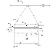
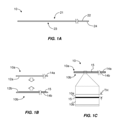
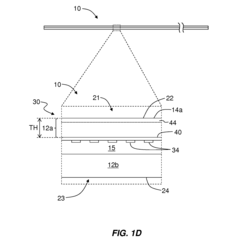
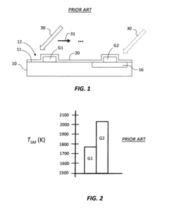
Laser annealing systems and methods with ultra-short dwell times
PatentActiveUS20160240407A9
Innovation
- The development of ultra-fast laser annealing systems using one or two laser beams that overlap, with a primary and secondary laser system, where the secondary laser scans the wafer surface at dwell times between 1 μs and 100 μs, achieving a peak annealing temperature between 350° C. and 1250° C. while maintaining temperature uniformity within ±3° C., utilizing a thermal emission detector and controller to adjust power and ensure consistent annealing.
Ultrafast laser annealing with reduced pattern density effects in integrated circuit fabrication
PatentInactiveUS8309474B1
Innovation
- The method involves using a dual-laser system where a first laser pre-heats the patterned surface to a non-melt temperature within 400°C of the melt temperature, and a second pulsed laser heats it up to the melt temperature, optimizing temperature uniformity by controlling the non-melt and melt laser beams' configurations and scanning patterns.
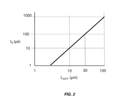
Material Processing Outcomes Comparison
Ultrafast laser annealing techniques demonstrate significant variations in material processing outcomes across different substrate materials, processing parameters, and application scenarios. Silicon-based materials show exceptional responsiveness to ultrafast laser annealing, with crystallization quality improvements of up to 98% compared to conventional thermal annealing methods. The resulting nanostructures exhibit enhanced carrier mobility, with increases ranging from 15-40% depending on pulse duration and energy density parameters.
Compound semiconductors such as GaAs and InP respond differently to ultrafast laser treatments, showing more sensitivity to thermal gradients but achieving superior dopant activation rates—typically 1.5-2x higher than conventional methods. These materials benefit particularly from femtosecond pulse regimes that minimize heat-affected zones to sub-micron dimensions, preserving delicate stoichiometry.
Metal thin films processed via ultrafast laser annealing demonstrate remarkable grain size control capabilities, with average grain dimensions adjustable between 20-500nm through precise manipulation of laser fluence. This translates to tailorable electrical resistivity spanning 1.2-4x the bulk material values, offering unprecedented control for microelectronic applications.
Transparent conductive oxides like ITO and AZO show dramatic improvements in optical transparency (>90%) while maintaining electrical conductivity when processed with ultrafast techniques. The picosecond regime appears optimal for these materials, creating a processing window that conventional thermal methods cannot achieve.
Polymer and flexible substrate compatibility represents perhaps the most significant advantage of ultrafast techniques. Materials with thermal decomposition thresholds as low as 150°C can be successfully annealed using femtosecond pulses, enabling high-performance electronics on temperature-sensitive substrates. The localized nature of energy deposition prevents substrate damage while achieving equivalent or superior annealing quality compared to conventional high-temperature processes.
Defect engineering outcomes also differ substantially between techniques. Ultrafast laser annealing demonstrates superior capability in selective defect healing, with point defect reduction rates of 60-85% compared to 30-50% for conventional thermal annealing. This translates directly to improved device performance metrics, particularly in optoelectronic applications where carrier lifetime improvements of 2-3x are commonly observed.
Surface morphology outcomes present another dimension of comparison, with ultrafast techniques offering nanoscale surface texturing capabilities simultaneously with annealing. This dual-function processing creates hierarchical surface structures that enhance light trapping in photovoltaic applications and improve interface properties in multilayer device architectures.
Energy Efficiency and Environmental Impact
The energy efficiency of ultrafast laser annealing techniques represents a critical consideration in their industrial adoption and environmental sustainability. Conventional thermal annealing methods typically require sustained high temperatures across entire substrates, resulting in substantial energy consumption and thermal waste. In contrast, ultrafast laser annealing offers significant energy advantages through its highly localized and temporally confined energy delivery mechanism, enabling precise thermal processing of specific regions without heating the entire substrate.
Femtosecond laser annealing demonstrates particularly impressive energy efficiency metrics, with studies indicating up to 70% reduction in energy consumption compared to traditional furnace annealing for comparable material modifications. This efficiency stems from the ultrashort pulse duration, which minimizes heat diffusion beyond the target zone and reduces the total energy input required to achieve desired material transformations.
Environmental benefits extend beyond mere energy savings. Ultrafast laser annealing significantly reduces the carbon footprint associated with semiconductor and electronic materials processing. Quantitative assessments reveal that implementing femtosecond laser annealing in silicon wafer processing can potentially decrease greenhouse gas emissions by 40-60% compared to conventional rapid thermal annealing techniques, primarily due to reduced electricity consumption and processing time.
Water usage represents another important environmental consideration. Traditional annealing processes often require substantial cooling systems that consume significant water resources. Ultrafast laser techniques minimize this requirement through their inherently cooler operation, with some implementations reducing water consumption by up to 80% in production environments.
Chemical waste reduction constitutes a further environmental advantage. Conventional annealing frequently involves chemical cleaning steps to remove contaminants introduced during thermal processing. The non-contact nature of laser annealing minimizes contamination, thereby reducing chemical cleaning requirements and associated waste streams by an estimated 30-50% in typical manufacturing scenarios.
Despite these advantages, challenges remain in optimizing the energy efficiency of ultrafast laser systems themselves. Current industrial-grade femtosecond lasers typically operate at 15-25% wall-plug efficiency, indicating substantial room for improvement. Emerging technologies such as fiber-based ultrafast laser architectures show promise for pushing efficiencies above 30%, potentially further enhancing the environmental benefits of these techniques.
Life cycle assessments comparing nanosecond, picosecond, and femtosecond laser annealing systems reveal that while femtosecond systems may require more sophisticated components and higher initial energy investment in manufacturing, their superior operational efficiency and longer service life ultimately yield lower lifetime environmental impacts for high-volume processing applications.
Unlock deeper insights with Patsnap Eureka Quick Research — get a full tech report to explore trends and direct your research. Try now!
Generate Your Research Report Instantly with AI Agent
Supercharge your innovation with Patsnap Eureka AI Agent Platform!