The Role of Ultrafast Laser Annealing in Electronic Device Fabrication
OCT 10, 202510 MIN READ
Generate Your Research Report Instantly with AI Agent
Patsnap Eureka helps you evaluate technical feasibility & market potential.
Ultrafast Laser Annealing Background and Objectives
Ultrafast laser annealing represents a significant technological advancement in the field of electronic device fabrication, emerging from decades of evolution in semiconductor processing techniques. This technology utilizes ultra-short laser pulses, typically in the femtosecond to picosecond range, to deliver precise thermal energy to semiconductor materials, enabling controlled modification of their structural and electrical properties without damaging surrounding areas.
The development of ultrafast laser annealing can be traced back to the 1980s when conventional thermal annealing methods began showing limitations in addressing the increasingly complex requirements of miniaturized electronic components. Traditional furnace annealing and rapid thermal processing (RTP) techniques faced challenges in achieving the spatial and temporal precision needed for advanced semiconductor devices, particularly as feature sizes approached the nanometer scale.
Throughout the 1990s and early 2000s, significant advancements in ultrafast laser technology, including the development of more stable and powerful femtosecond laser sources, paved the way for their application in semiconductor processing. The ability to deliver extremely short pulses with high peak powers allowed for unprecedented control over the annealing process, minimizing thermal diffusion and enabling highly localized treatment of materials.
The technological evolution continued with improvements in beam shaping, pulse control, and integration with automated manufacturing systems, making ultrafast laser annealing increasingly viable for industrial applications. Recent years have witnessed the refinement of these techniques to address specific challenges in advanced electronic device fabrication, including activation of dopants, crystallization of amorphous materials, and defect engineering in novel semiconductor compounds.
The primary objective of ultrafast laser annealing technology is to achieve precise modification of material properties while maintaining the integrity of surrounding structures, a critical requirement as device dimensions continue to shrink. Specifically, this technology aims to enable effective dopant activation, improve carrier mobility, reduce leakage currents, and enhance overall device performance through controlled thermal processing at the nanoscale.
Additional objectives include developing scalable and cost-effective processes suitable for high-volume manufacturing, ensuring compatibility with emerging materials and device architectures, and reducing the environmental impact associated with traditional annealing methods. The technology also seeks to address the growing demand for flexible electronics and three-dimensional integrated circuits, where conventional thermal processing techniques face significant limitations.
Looking forward, ultrafast laser annealing technology is expected to play an increasingly crucial role in enabling the continued advancement of semiconductor devices according to Moore's Law, particularly as the industry transitions to sub-5nm nodes and explores novel materials and architectures beyond traditional silicon-based technologies.
Market Demand Analysis for Advanced Electronic Fabrication
The global market for advanced electronic fabrication technologies is experiencing unprecedented growth, driven by the increasing demand for smaller, faster, and more energy-efficient electronic devices. Ultrafast laser annealing has emerged as a critical technology in this landscape, addressing key manufacturing challenges in semiconductor and microelectronics production. The market size for advanced electronic fabrication equipment is projected to reach $103 billion by 2026, with laser-based processing technologies accounting for approximately 18% of this market.
Consumer electronics continues to be the primary driver of demand, with smartphones, tablets, and wearable devices requiring increasingly sophisticated semiconductor components. The transition to 5G technology has further accelerated this trend, creating demand for high-performance RF components that benefit from precise annealing processes. Industry analysts estimate that over 70% of premium smartphones will incorporate components manufactured using advanced annealing techniques by 2025.
The automotive sector represents another significant market, particularly with the rapid growth of electric vehicles and autonomous driving systems. These applications require high-reliability electronic components that can withstand harsh operating conditions, creating demand for the superior material properties achieved through ultrafast laser annealing. The automotive semiconductor market is growing at 12% annually, with advanced manufacturing processes becoming increasingly important.
Industrial IoT applications are expanding rapidly, with an estimated 75 billion connected devices expected by 2025. This proliferation of edge computing devices creates substantial demand for energy-efficient processors and sensors, many of which benefit from the precise thermal control offered by ultrafast laser annealing during fabrication.
Regional analysis reveals that East Asia dominates the market for advanced electronic fabrication, with China, Taiwan, South Korea, and Japan collectively accounting for over 65% of global semiconductor manufacturing capacity. However, recent geopolitical tensions have accelerated efforts to diversify supply chains, with significant investments in new fabrication facilities in North America and Europe.
Market research indicates that manufacturers are increasingly prioritizing sustainable manufacturing processes, with energy efficiency and reduced chemical waste being key considerations. Ultrafast laser annealing offers advantages in this regard, consuming significantly less energy than conventional furnace-based annealing while eliminating the need for certain chemical processes.
The COVID-19 pandemic has highlighted vulnerabilities in global supply chains, leading to increased investment in advanced manufacturing technologies that can enable more resilient and localized production capabilities. This trend is expected to further accelerate adoption of flexible manufacturing technologies like ultrafast laser annealing.
Current State and Challenges in Laser Annealing Technology
Ultrafast laser annealing technology has emerged as a critical process in modern electronic device fabrication, with significant advancements achieved globally. Currently, the technology has matured to enable precise thermal processing at the nanoscale, allowing for controlled modification of material properties without damaging surrounding structures. In the United States and Europe, research institutions have developed systems capable of sub-picosecond pulse durations with peak powers exceeding several terawatts, facilitating unprecedented control over the annealing process.
In Asia, particularly in Japan, South Korea, and Taiwan, industrial implementation has accelerated, with major semiconductor manufacturers integrating ultrafast laser annealing into production lines for advanced node processes. These regions have demonstrated particular expertise in scaling the technology for high-volume manufacturing environments while maintaining process stability and yield.
Despite these advancements, several significant challenges persist in ultrafast laser annealing technology. The primary technical hurdle remains the difficulty in achieving uniform thermal profiles across large wafer areas. Current systems exhibit spatial variations in energy distribution that can lead to inconsistent annealing results, particularly problematic as device dimensions continue to shrink below 5nm nodes.
Another critical challenge is the complex interaction between ultrafast laser pulses and increasingly diverse material stacks used in modern semiconductor devices. The presence of multiple thin films with varying optical and thermal properties creates unpredictable energy absorption patterns, making process optimization highly complex and often empirical rather than theoretical.
The integration of real-time monitoring and feedback systems represents another technological gap. Current systems typically operate in an open-loop configuration, lacking the sophisticated in-situ measurement capabilities necessary to adjust processing parameters dynamically during the annealing process. This limitation restricts the ability to compensate for material variations or equipment drift.
From a manufacturing perspective, throughput limitations continue to constrain widespread adoption. The sequential nature of laser scanning processes creates bottlenecks in high-volume production environments, with current systems processing significantly fewer wafers per hour compared to conventional rapid thermal annealing technologies.
Cost considerations also present significant barriers to implementation. The high capital expenditure required for ultrafast laser systems, combined with specialized maintenance requirements and limited supplier ecosystems, creates economic challenges for manufacturers considering technology adoption. This is particularly acute for smaller fabrication facilities without the economies of scale enjoyed by industry leaders.
Addressing these challenges will require interdisciplinary collaboration between laser physics experts, materials scientists, and process engineers to develop next-generation solutions that can overcome current limitations while meeting the increasingly demanding requirements of advanced electronic device fabrication.
Current Ultrafast Laser Annealing Implementation Methods
01 Semiconductor device manufacturing using ultrafast laser annealing
Ultrafast laser annealing is used in semiconductor manufacturing to modify material properties without causing thermal damage to surrounding areas. The technique employs femtosecond or picosecond lasers to precisely anneal specific regions of semiconductor wafers, enabling the creation of high-performance electronic devices. This process allows for localized heating and rapid cooling, which is crucial for advanced node semiconductor fabrication where precise control of dopant activation and crystal structure is required.- Semiconductor device manufacturing using ultrafast laser annealing: Ultrafast laser annealing is utilized in semiconductor manufacturing processes to modify material properties with minimal thermal damage. The technique employs femtosecond or picosecond laser pulses to precisely anneal semiconductor materials, enabling better control over dopant activation, crystallization, and defect reduction. This approach allows for localized heating without affecting surrounding areas, making it ideal for advanced semiconductor device fabrication where thermal budget constraints are critical.
- Laser parameters optimization for ultrafast annealing: Optimizing laser parameters is crucial for effective ultrafast laser annealing processes. This includes controlling pulse duration, repetition rate, wavelength, and energy density to achieve desired material modifications. By precisely tuning these parameters, manufacturers can optimize the annealing process for specific materials and applications, resulting in improved material properties while minimizing thermal damage and unwanted effects. The optimization process often involves sophisticated modeling and real-time monitoring systems.
- Materials processing applications of ultrafast laser annealing: Ultrafast laser annealing has diverse applications in materials processing beyond semiconductors. It can be used for surface modification of metals, ceramics, and polymers to enhance properties like hardness, wear resistance, and corrosion protection. The technique enables precise microstructural changes, nanoparticle formation, and controlled phase transformations. These capabilities make ultrafast laser annealing valuable for manufacturing advanced materials with tailored properties for specific industrial applications.
- Optical and photonic device fabrication using ultrafast laser annealing: Ultrafast laser annealing plays a significant role in fabricating optical and photonic devices. The technique enables precise modification of optical materials to create waveguides, gratings, and other photonic structures. By controlling the refractive index changes through localized annealing, manufacturers can produce high-performance optical components with minimal defects. This approach is particularly valuable for integrated photonics, fiber optics, and optoelectronic device manufacturing where nanoscale precision is required.
- Medical and biological applications of ultrafast laser annealing: Ultrafast laser annealing has emerging applications in medical and biological fields. The technique enables precise modification of biomaterials, creation of biocompatible surfaces, and controlled drug delivery systems. In medical device manufacturing, ultrafast laser annealing can be used to modify implant surfaces for improved biocompatibility and functionality. The non-thermal nature of ultrafast processes minimizes damage to sensitive biological materials, making it suitable for applications where preserving biological activity is crucial.
02 Ultrafast laser annealing for optical materials and photonics
Ultrafast laser annealing techniques are applied to optical materials and photonic components to modify their optical properties. This process involves using short-pulse lasers to induce controlled changes in refractive index, optical absorption, or other properties without causing bulk heating. Applications include the fabrication of optical waveguides, fiber Bragg gratings, and other integrated photonic components. The precise energy deposition of ultrafast lasers allows for three-dimensional modifications within transparent materials.Expand Specific Solutions03 Material processing and surface modification via ultrafast laser annealing
Ultrafast laser annealing enables precise surface modification and material processing across various substrates. The technique allows for controlled texturing, hardening, or functionalization of surfaces without affecting the bulk material properties. The extremely short pulse duration minimizes the heat-affected zone, resulting in high-precision surface treatments. This approach is particularly valuable for creating specialized surface properties such as enhanced hydrophobicity, improved wear resistance, or modified optical characteristics.Expand Specific Solutions04 Ultrafast laser annealing systems and equipment design
Specialized equipment and systems have been developed for ultrafast laser annealing applications. These systems incorporate advanced beam delivery optics, precise positioning stages, and sophisticated control software to achieve the required processing precision. Key innovations include beam shaping technologies, pulse control mechanisms, and real-time monitoring systems that ensure consistent annealing results. The design of these systems focuses on maintaining beam quality, ensuring pulse stability, and providing the flexibility needed for various industrial applications.Expand Specific Solutions05 Medical and biological applications of ultrafast laser annealing
Ultrafast laser annealing has found applications in medical and biological fields, particularly in tissue modification and medical device manufacturing. The precise energy deposition allows for controlled tissue ablation with minimal thermal damage to surrounding areas, making it suitable for delicate procedures. Additionally, the technique is used in the fabrication of biomedical implants and devices where precise material modifications are required. The non-thermal nature of ultrafast laser processing helps preserve the biocompatibility of treated materials.Expand Specific Solutions
Key Industry Players in Ultrafast Laser Systems
The ultrafast laser annealing market in electronic device fabrication is currently in a growth phase, with increasing adoption across semiconductor manufacturing. The global market is expanding rapidly, driven by demands for higher performance electronic devices and more efficient manufacturing processes. Technologically, companies like Applied Materials, Veeco Instruments, and Ultratech lead with mature solutions, while Coherent and Gigaphoton demonstrate strong capabilities in laser source technology. Asian manufacturers including SMIC, Samsung Display, and Japan Display are integrating these technologies into production lines. Emerging players like Shanghai Micro Electronics Equipment and Beijing U-PRECISION TECH are developing competitive solutions, indicating the technology's transition from specialized application to mainstream manufacturing process, particularly for advanced semiconductor and display fabrication.
Semiconductor Energy Laboratory Co., Ltd.
Technical Solution: Semiconductor Energy Laboratory (SEL) has developed proprietary ultrafast laser annealing technology specifically for thin-film transistor (TFT) fabrication. Their approach utilizes picosecond and femtosecond lasers to crystallize amorphous silicon films into high-quality polycrystalline silicon with precisely controlled grain structures. SEL's technology employs a unique optical system that shapes the laser beam into a linear profile with carefully engineered intensity distribution, enabling uniform crystallization across large areas essential for display manufacturing[5]. Their process achieves carrier mobilities exceeding 100 cm²/Vs in polycrystalline silicon films, significantly higher than conventional solid-phase crystallization methods. SEL has further refined their ULA technology to work with oxide semiconductor materials, particularly IGZO (Indium Gallium Zinc Oxide), where ultrafast laser annealing is used to optimize the semiconductor-insulator interface properties without damaging the temperature-sensitive oxide layers[6]. This has enabled the development of high-performance, low-power oxide TFTs suitable for next-generation displays and flexible electronics.
Strengths: Unparalleled expertise in laser crystallization for display applications; demonstrated success in mass production environments; proprietary beam shaping technology for uniform processing. Weaknesses: Technology primarily optimized for display applications rather than general semiconductor processing; requires precise control of ambient conditions during processing; higher initial investment compared to conventional annealing methods.
Sony Group Corp.
Technical Solution: Sony has developed advanced ultrafast laser annealing technology primarily focused on applications in image sensor fabrication and display manufacturing. Their approach utilizes proprietary femtosecond laser systems with pulse durations below 200fs and sophisticated beam delivery optics that enable precise energy deposition in multilayer device structures. Sony's ULA technology has been particularly successful in backside-illuminated CMOS image sensor fabrication, where ultrafast laser annealing is used to activate dopants in the silicon while preserving the integrity of temperature-sensitive metal interconnects and optical structures[9]. The company has also pioneered the use of ultrafast laser annealing for crystallization of amorphous silicon films in high-performance displays, achieving grain sizes exceeding 10μm with highly controlled orientation - critical for high-mobility TFTs in premium display products. Sony's systems incorporate advanced beam homogenization techniques that ensure uniform energy distribution across large processing areas, enabling consistent device performance across the entire substrate. Their latest generation technology utilizes spatial light modulators to create customized beam profiles optimized for specific device architectures, allowing unprecedented control over the thermal profile during the annealing process[10].
Strengths: Exceptional precision in energy delivery for complex multilayer structures; demonstrated success in mass production of premium consumer electronics; advanced beam shaping capabilities for application-specific optimization. Weaknesses: Proprietary technology primarily developed for internal use rather than equipment sales; limited public information on specific process parameters; higher implementation costs compared to conventional annealing methods.
Core Innovations in Ultrafast Laser-Material Interactions
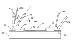
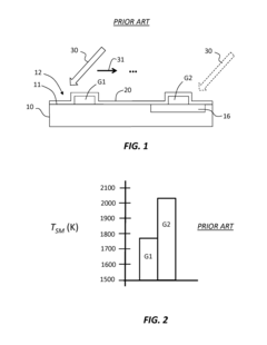
Ultrafast laser annealing with reduced pattern density effects in integrated circuit fabrication
PatentInactiveUS20140097171A1
Innovation
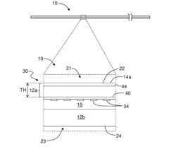
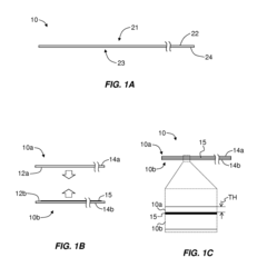
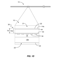
- The method involves using a dual-laser system where a first laser heats the patterned surface to a non-melt temperature within 400°C of the melt temperature, and a second pulsed laser further heats it to the melt temperature, optimizing temperature uniformity and reducing pattern density effects through controlled heat diffusion.
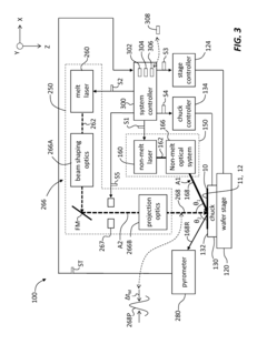
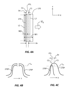
Laser annealing systems and methods with ultra-short dwell times
PatentActiveUS20160240407A9
Innovation
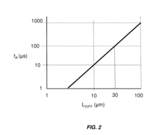
- The development of ultra-fast laser annealing systems using one or two laser beams that overlap, with a primary and secondary laser system, where the secondary laser scans the wafer surface at dwell times between 1 μs and 100 μs, achieving a peak annealing temperature between 350° C. and 1250° C. while maintaining temperature uniformity within ±3° C., utilizing a thermal emission detector and controller to adjust power and ensure consistent annealing.
Energy Efficiency and Sustainability Considerations
Ultrafast laser annealing represents a significant advancement in electronic device fabrication technology, offering substantial energy efficiency benefits compared to conventional thermal annealing methods. Traditional annealing processes typically require heating entire substrates or wafers to high temperatures for extended periods, consuming considerable energy and creating thermal stress throughout the material. In contrast, ultrafast laser annealing delivers precisely targeted energy only where needed, dramatically reducing the overall energy footprint of the manufacturing process.
The localized nature of ultrafast laser processing minimizes waste heat generation, with energy savings estimated between 30-60% compared to conventional furnace annealing, depending on the specific application. This efficiency stems from the ultrashort pulse duration (femtoseconds to picoseconds), which allows for rapid energy transfer to the target material without significant thermal diffusion to surrounding areas.
From a sustainability perspective, ultrafast laser annealing contributes to greener electronics manufacturing through several mechanisms. The reduced energy consumption directly translates to lower carbon emissions associated with device fabrication. Additionally, the precise nature of the process minimizes material waste through more efficient dopant activation and defect repair, extending the lifespan of electronic components and reducing the environmental impact of electronic waste.
Water usage represents another critical sustainability consideration. Conventional annealing processes often require substantial cooling systems that consume significant water resources. Ultrafast laser annealing's minimal heat generation substantially reduces cooling requirements, with some implementations demonstrating water usage reductions of up to 40% compared to traditional methods.
The technology also enables the processing of temperature-sensitive materials that would be damaged by conventional thermal treatments, opening pathways for more environmentally friendly substrate materials and flexible electronics. This compatibility with novel materials supports the development of biodegradable electronics and components with reduced environmental footprints.
Looking forward, ongoing research aims to further enhance the energy efficiency of ultrafast laser annealing systems. Developments in laser source technology are steadily improving wall-plug efficiency, while advanced beam delivery systems and process optimization algorithms are maximizing energy transfer efficiency. These improvements collectively position ultrafast laser annealing as a cornerstone technology for sustainable semiconductor manufacturing in alignment with global carbon reduction targets and environmental regulations.
Integration with Industry 4.0 Manufacturing Systems
The integration of ultrafast laser annealing technology with Industry 4.0 manufacturing systems represents a significant advancement in electronic device fabrication. This convergence creates a synergistic relationship where the precision and efficiency of ultrafast laser annealing can be fully leveraged through smart manufacturing principles, data analytics, and interconnected production systems.
Industry 4.0 frameworks provide the digital infrastructure necessary to optimize ultrafast laser annealing processes through real-time monitoring and adaptive control systems. By implementing IoT sensors throughout the annealing process, manufacturers can collect comprehensive data on laser parameters, substrate temperatures, and material responses. This data stream enables continuous process optimization and quality control that was previously unattainable in traditional manufacturing environments.
Machine learning algorithms integrated with ultrafast laser annealing systems can predict optimal processing parameters based on material characteristics and desired device specifications. These predictive capabilities significantly reduce setup times and material waste while increasing throughput and yield rates. The self-learning nature of these systems allows for continuous improvement in annealing protocols without human intervention.
Digital twin technology offers particularly promising applications for ultrafast laser annealing integration. By creating virtual replicas of the annealing process, engineers can simulate various scenarios and optimize parameters before physical implementation. This capability is especially valuable when working with novel materials or complex device architectures where experimental approaches would be costly and time-consuming.
The implementation of cyber-physical systems enables seamless coordination between ultrafast laser annealing equipment and other fabrication processes. This horizontal integration ensures that annealing steps are perfectly timed within the broader manufacturing workflow, reducing bottlenecks and idle time. Vertical integration with enterprise resource planning systems further optimizes material flow and production scheduling.
Cloud-based manufacturing platforms can facilitate the sharing of ultrafast laser annealing expertise across global manufacturing networks. This democratization of advanced processing knowledge accelerates innovation and enables smaller manufacturers to implement cutting-edge annealing techniques that were previously accessible only to large corporations with extensive R&D resources.
Augmented reality interfaces provide operators with enhanced visualization of the annealing process, displaying real-time data overlays and step-by-step guidance. This technology bridges the knowledge gap between expert engineers and production staff, ensuring consistent implementation of complex annealing protocols across different manufacturing facilities and shifts.
Unlock deeper insights with Patsnap Eureka Quick Research — get a full tech report to explore trends and direct your research. Try now!
Generate Your Research Report Instantly with AI Agent
Supercharge your innovation with Patsnap Eureka AI Agent Platform!