Understanding Ultrafast Laser Annealing in Semiconductor Fabrication
OCT 10, 202510 MIN READ
Generate Your Research Report Instantly with AI Agent
Patsnap Eureka helps you evaluate technical feasibility & market potential.
Ultrafast Laser Annealing Background and Objectives
Ultrafast laser annealing (ULA) represents a significant advancement in semiconductor fabrication technology, evolving from conventional thermal annealing methods that have been fundamental to semiconductor manufacturing since the 1960s. The technology utilizes ultra-short laser pulses in the femtosecond to picosecond range to selectively heat semiconductor materials with unprecedented spatial and temporal precision. This evolution addresses critical limitations in traditional annealing techniques, particularly as semiconductor device dimensions continue to shrink below 10nm.
The historical trajectory of annealing technologies in semiconductor fabrication reveals a consistent push toward more precise thermal control and reduced thermal budgets. From furnace annealing to rapid thermal processing (RTP), and subsequently to millisecond annealing techniques like flash lamp annealing (FLA), each advancement has enabled finer control over dopant activation and defect repair while minimizing unwanted diffusion. Ultrafast laser annealing represents the latest milestone in this progression, offering sub-microsecond processing times and nanoscale spatial resolution.
Current technological trends indicate a growing emphasis on advanced materials integration, three-dimensional device architectures, and heterogeneous integration in semiconductor manufacturing. These developments necessitate annealing solutions capable of addressing complex thermal requirements across diverse material systems while maintaining atomic-level precision. ULA's ability to deliver highly localized energy with minimal thermal diffusion positions it as a potentially transformative technology in this landscape.
The primary objectives of ultrafast laser annealing research and development center on several key areas. First, achieving precise control over dopant activation while minimizing diffusion, which is critical for maintaining ultra-shallow junctions in advanced logic devices. Second, enabling defect engineering with nanoscale precision to optimize carrier mobility and reduce leakage currents. Third, facilitating novel material integration by providing tailored thermal processing solutions for emerging semiconductor materials such as III-V compounds, 2D materials, and wide-bandgap semiconductors.
Additionally, ULA aims to support advanced packaging technologies by enabling selective annealing of interconnect structures without compromising temperature-sensitive components. The technology also seeks to enhance manufacturing efficiency through reduced thermal budgets and processing times, potentially enabling single-wafer processing with high throughput. These objectives align with the semiconductor industry's roadmap toward more powerful, energy-efficient devices with increasingly complex architectures.
The ultimate goal of ultrafast laser annealing development is to establish a versatile, precise thermal processing platform that can address the multifaceted challenges of next-generation semiconductor fabrication, supporting continued scaling according to Moore's Law while enabling new device paradigms beyond traditional CMOS technology.
Semiconductor Market Demand Analysis
The semiconductor industry is experiencing unprecedented growth, with the global market projected to reach $1 trillion by 2030, driven primarily by increasing demand for advanced processing capabilities in emerging technologies. Within this expanding landscape, ultrafast laser annealing represents a critical enabling technology that addresses several key market demands across multiple semiconductor application segments.
Consumer electronics continues to be a primary driver, with smartphone manufacturers requiring increasingly sophisticated semiconductor components that deliver higher performance while maintaining energy efficiency. The miniaturization trend in consumer devices necessitates more precise fabrication techniques, where ultrafast laser annealing offers significant advantages over conventional thermal processing methods.
The automotive sector presents another substantial growth area, with the average semiconductor content per vehicle increasing dramatically as advanced driver-assistance systems (ADAS) and electric vehicle technologies become mainstream. These applications demand semiconductors with exceptional reliability and performance characteristics that ultrafast laser annealing can help deliver through improved dopant activation and reduced defect formation.
Data centers and cloud computing infrastructure represent a particularly high-growth segment, with global data center semiconductor demand growing at approximately 15% annually. These applications require high-performance logic chips that benefit significantly from the precise thermal control offered by ultrafast laser annealing techniques.
The emerging artificial intelligence and machine learning markets are creating unprecedented demand for specialized semiconductor components. These applications require chips with extremely high transistor densities and sophisticated architectures that push conventional fabrication techniques to their limits. Ultrafast laser annealing offers potential solutions to the thermal management challenges inherent in these advanced designs.
From a geographic perspective, East Asia continues to dominate semiconductor manufacturing, with significant investments in advanced fabrication capabilities. However, recent supply chain disruptions have accelerated efforts to diversify manufacturing locations, with major initiatives underway in North America and Europe that will likely incorporate cutting-edge processes including ultrafast laser annealing.
The Internet of Things (IoT) ecosystem represents another significant market driver, with billions of connected devices requiring specialized semiconductor components. Many IoT applications demand low-power, high-reliability semiconductors that can benefit from the precise dopant activation and reduced thermal budget offered by ultrafast laser annealing techniques.
Overall market analysis indicates that technologies enabling higher performance, improved energy efficiency, and enhanced reliability will command premium positions in the semiconductor value chain, positioning ultrafast laser annealing as a strategically important capability for manufacturers seeking competitive advantage in high-value market segments.
Current Ultrafast Laser Technology Challenges
Despite significant advancements in ultrafast laser annealing technology for semiconductor fabrication, several critical challenges persist that limit its widespread industrial adoption. The primary technical hurdle remains the precise control of energy deposition during the ultrashort pulse duration (typically femtoseconds to picoseconds). This challenge is particularly acute when processing advanced semiconductor materials with varying absorption properties and thermal conductivities.
Thermal gradient management presents another significant obstacle. The extremely rapid heating and cooling rates (>10^10 K/s) create steep thermal gradients that can induce mechanical stress and potential damage to delicate nanostructures. Engineers continue to struggle with developing models that accurately predict these thermal behaviors across different material systems and device architectures.
Beam profile uniformity and stability represent persistent challenges for industrial implementation. Current ultrafast laser systems often exhibit pulse-to-pulse energy variations and spatial beam inhomogeneities that can lead to processing inconsistencies across large wafer areas. This becomes increasingly problematic as semiconductor feature sizes continue to shrink below 5nm, where even minor processing variations can significantly impact device performance.
Integration with existing semiconductor manufacturing workflows poses substantial engineering challenges. Ultrafast laser annealing systems require sophisticated beam delivery optics, precise positioning stages, and complex control systems that must operate reliably in clean room environments. The development of robust, maintenance-friendly systems that meet semiconductor industry standards for throughput and reliability remains an ongoing challenge.
Real-time monitoring and process control capabilities are currently insufficient for high-volume manufacturing applications. Unlike conventional thermal annealing methods, ultrafast laser processes occur too rapidly for conventional temperature monitoring techniques. This creates difficulties in implementing closed-loop control systems necessary for ensuring consistent processing results across production runs.
Cost considerations continue to impede widespread adoption. Current ultrafast laser systems suitable for semiconductor processing typically cost several million dollars, with additional expenses for specialized optics, beam delivery systems, and maintenance. The economic justification for this investment versus established annealing technologies remains challenging for many applications, particularly in cost-sensitive market segments.
Material-specific optimization represents another significant challenge. Different semiconductor materials and device structures require tailored laser parameters (wavelength, pulse duration, energy density) to achieve optimal results. Developing a comprehensive understanding of these material-specific responses and creating flexible processing platforms capable of addressing diverse material requirements continues to challenge researchers and equipment manufacturers.
Current Ultrafast Laser Annealing Solutions
01 Semiconductor device manufacturing using ultrafast laser annealing
Ultrafast laser annealing is applied in semiconductor manufacturing processes to modify material properties without causing thermal damage to surrounding areas. The technique uses femtosecond or picosecond laser pulses to precisely anneal specific regions of semiconductor wafers, enabling improved device performance. This method allows for selective doping activation, crystallization of amorphous silicon, and defect repair in semiconductor structures while maintaining the integrity of temperature-sensitive components nearby.- Semiconductor device manufacturing using ultrafast laser annealing: Ultrafast laser annealing is used in semiconductor manufacturing to modify material properties without causing thermal damage to surrounding areas. The process involves using ultrashort laser pulses to rapidly heat and cool semiconductor materials, enabling precise doping, crystallization, and defect repair. This technique is particularly valuable for advanced node technologies where precise thermal control is critical for maintaining device integrity and performance.
- Materials processing with ultrafast laser annealing: Ultrafast laser annealing enables sophisticated materials processing capabilities across various substrates including metals, glasses, and polymers. The technique allows for precise modification of material properties through controlled energy deposition that can alter crystalline structures, improve electrical conductivity, or enhance optical properties. The non-equilibrium heating and cooling dynamics of ultrafast laser annealing create unique material phases and structures not achievable with conventional thermal processing methods.
- Optical device fabrication using ultrafast laser annealing: Ultrafast laser annealing is employed in the fabrication of optical devices such as waveguides, photonic integrated circuits, and optical sensors. The technique enables precise modification of refractive indices in transparent materials, creation of optical gratings, and formation of active optical regions. By controlling the laser parameters, manufacturers can tailor the optical properties of materials with nanoscale precision, enabling advanced photonic components with enhanced functionality.
- Advanced laser systems for ultrafast annealing applications: Specialized laser systems have been developed specifically for ultrafast annealing applications. These systems typically feature high repetition rates, precise pulse control, and beam shaping capabilities to optimize the annealing process. Key innovations include synchronization systems for multi-beam processing, adaptive optics for beam quality enhancement, and sophisticated monitoring systems that enable real-time process control. These advanced laser systems enable industrial-scale implementation of ultrafast annealing for various manufacturing applications.
- Medical and biological applications of ultrafast laser annealing: Ultrafast laser annealing has found applications in medical and biological fields, including tissue modification, drug delivery systems, and biomedical device fabrication. The technique's ability to deliver precise energy without thermal damage to surrounding areas makes it suitable for delicate biological materials. Applications include surface modification of implantable devices, controlled release mechanisms for pharmaceuticals, and creation of microstructures for cell culture and tissue engineering.
02 Ultrafast laser annealing for material processing and modification
Ultrafast laser annealing techniques are employed for various material processing applications, including surface modification, nanostructure formation, and property enhancement of different materials. The extremely short pulse duration allows for precise energy deposition, minimizing heat-affected zones and enabling unique material transformations. This approach can be used to modify optical, electrical, and mechanical properties of materials through controlled melting and resolidification processes without bulk heating.Expand Specific Solutions03 Optical device fabrication using ultrafast laser annealing
Ultrafast laser annealing is utilized in the fabrication and modification of optical devices such as waveguides, photonic integrated circuits, and optical fibers. The technique enables precise refractive index modification, waveguide writing, and optical property tuning through localized heating and rapid quenching. This approach allows for three-dimensional optical structure formation within transparent materials and can be used to create complex photonic devices with minimal thermal damage to surrounding regions.Expand Specific Solutions04 Medical and biological applications of ultrafast laser annealing
Ultrafast laser annealing has applications in medical and biological fields, including tissue modification, drug delivery systems, and biomedical device fabrication. The precise energy control of ultrafast lasers allows for targeted treatment of biological materials with minimal collateral damage. This technique can be used for controlled tissue ablation, modification of implantable medical devices, and creation of microstructures for biological applications while preserving surrounding sensitive tissues.Expand Specific Solutions05 Advanced laser systems and control methods for ultrafast annealing
Specialized laser systems and control methodologies have been developed specifically for ultrafast laser annealing applications. These systems incorporate precise pulse shaping, beam steering, and monitoring technologies to achieve controlled energy deposition. Advanced techniques include spatial and temporal pulse shaping, beam homogenization, and real-time process monitoring to ensure uniform annealing results. These developments enable more precise control over the annealing process, allowing for optimization of material transformations across various applications.Expand Specific Solutions
Key Industry Players in Laser Processing
Ultrafast Laser Annealing in semiconductor fabrication is currently in a growth phase, with the market expanding rapidly due to increasing demand for advanced semiconductor manufacturing processes. The global market size is estimated to reach several billion dollars by 2025, driven by applications in high-performance chip production. Technologically, the field is approaching maturity with key players demonstrating varied capabilities. Companies like Samsung Electronics, Taiwan Semiconductor Manufacturing Co., and Veeco Instruments lead with commercial implementations, while Semiconductor Energy Laboratory and EO Technics offer specialized solutions. Research institutions including Kyushu University and University of Electronic Science & Technology of China are advancing fundamental technologies. Emerging players such as Beijing U-PRECISION TECH and Shanghai Micro Electronics Equipment are developing competitive alternatives, indicating a diversifying ecosystem with both established and new entrants competing for market share.
Gigaphoton, Inc.
Technical Solution: Gigaphoton has developed an advanced ultrafast laser annealing platform utilizing their expertise in high-power excimer laser technology. Their system employs a KrF excimer laser operating at 248nm wavelength with pulse durations in the nanosecond range, enabling extremely shallow absorption depths ideal for surface processing of semiconductor materials. Gigaphoton's technology incorporates a proprietary beam homogenization system that achieves energy uniformity better than ±2% across the processing area. Their approach features a multi-pulse methodology where thousands of precisely controlled laser pulses are delivered to gradually heat the target material, allowing for unprecedented control over the thermal profile. The company has developed specialized optical systems that can project patterned laser energy distributions, enabling selective annealing of specific device regions. Gigaphoton's technology has been particularly effective for ultra-shallow junction formation in advanced logic devices, crystallization of high-k dielectric materials, and interface engineering in heterogeneous semiconductor structures[8][10].
Strengths: Exceptional control over annealing depth due to short wavelength; capability for selective area processing; minimal thermal impact on underlying layers. Weaknesses: Lower throughput compared to scanning-based systems; higher maintenance requirements for excimer laser sources; more complex integration with existing process flows.
Veeco Instruments, Inc.
Technical Solution: Veeco has developed the LSA101 Laser Spike Annealing system specifically designed for advanced semiconductor manufacturing. Their technology utilizes a high-power continuous wave laser that is rapidly scanned across the wafer surface, creating a controlled temperature profile with extremely fast ramp rates. The system employs proprietary beam shaping optics that transform the Gaussian laser beam into a highly uniform line beam with length-to-width ratios exceeding 100:1. Veeco's technology incorporates advanced thermal modeling algorithms that predict and compensate for edge effects and pattern density variations across the wafer. Their latest systems feature dual-beam capability, where a pre-heating laser works in conjunction with the main annealing laser to optimize temperature profiles and reduce thermal stress. Veeco has demonstrated successful implementation of their technology for dopant activation in sub-10nm devices, nickel silicide formation for advanced contacts, and defect engineering in strained silicon structures[7][9].
Strengths: Excellent control over temperature gradients; compatible with a wide range of wafer sizes; sophisticated thermal modeling capabilities for process optimization. Weaknesses: Higher initial capital investment compared to conventional annealing equipment; requires specialized operator training; challenges in processing wafers with significant topography.
Core Patents and Research in Ultrafast Annealing
Laser annealing systems and methods with ultra-short dwell times
PatentActiveUS20160240407A9
Innovation
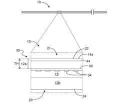
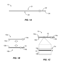
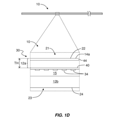
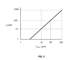
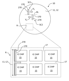
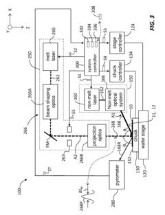
- The development of ultra-fast laser annealing systems using one or two laser beams that overlap, with a primary and secondary laser system, where the secondary laser scans the wafer surface at dwell times between 1 μs and 100 μs, achieving a peak annealing temperature between 350° C. and 1250° C. while maintaining temperature uniformity within ±3° C., utilizing a thermal emission detector and controller to adjust power and ensure consistent annealing.
Ultrafast laser annealing with reduced pattern density effects in integrated circuit fabrication
PatentInactiveUS8309474B1
Innovation
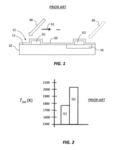
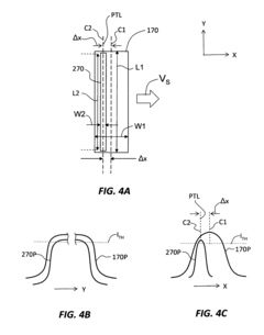
- The method involves using a dual-laser system where a first laser pre-heats the patterned surface to a non-melt temperature within 400°C of the melt temperature, and a second pulsed laser heats it up to the melt temperature, optimizing temperature uniformity by controlling the non-melt and melt laser beams' configurations and scanning patterns.
Environmental Impact Assessment
Ultrafast laser annealing in semiconductor fabrication presents significant environmental considerations that must be evaluated against traditional thermal annealing methods. The process demonstrates notable environmental advantages through reduced energy consumption, with ultrafast laser systems requiring substantially less power than conventional furnace-based annealing equipment. This efficiency stems from the targeted nature of laser processing, which heats only specific substrate regions rather than entire wafers or batches, resulting in energy savings of up to 40-60% compared to conventional methods.
The reduction in process chemicals represents another environmental benefit. Ultrafast laser annealing minimizes or eliminates the need for certain wet chemical processes traditionally used in semiconductor manufacturing. Studies indicate a potential reduction of hazardous chemical usage by 15-30%, decreasing both environmental contamination risks and waste management requirements.
Waste reduction outcomes are equally significant. The precise nature of ultrafast laser processing generates less material waste through improved yield rates and reduced defect formation. Industry data suggests that advanced laser annealing techniques can improve material utilization efficiency by 10-25%, directly translating to less semiconductor waste entering landfills or requiring specialized disposal.
Carbon footprint analysis reveals that facilities implementing ultrafast laser annealing can achieve meaningful greenhouse gas emission reductions. When accounting for both direct energy consumption and indirect emissions from chemical production and waste management, total carbon footprint reductions of 20-35% have been documented in manufacturing facilities that have transitioned to laser-based processes.
Water conservation represents another environmental advantage, as ultrafast laser annealing typically requires less cooling water than conventional thermal processes. Manufacturing facilities implementing these advanced techniques have reported water usage reductions of 15-30% in their annealing operations, contributing to overall industrial water conservation efforts.
However, challenges remain regarding equipment lifecycle considerations. The specialized optics and precision components in ultrafast laser systems contain rare earth elements and specialized materials that present recycling and disposal challenges. Current research focuses on developing more environmentally sustainable laser system components and establishing effective recycling protocols for end-of-life equipment.
Regulatory compliance frameworks are evolving to address these new technologies. Semiconductor manufacturers implementing ultrafast laser annealing must navigate changing environmental regulations, particularly regarding energy efficiency standards, chemical use restrictions, and electronic waste management. Leading manufacturers are proactively developing environmental management systems that exceed current compliance requirements in anticipation of stricter future regulations.
Integration with Advanced Node Manufacturing
The integration of ultrafast laser annealing (ULA) with advanced node manufacturing represents a critical frontier in semiconductor fabrication technology. As process nodes continue to shrink below 5nm, traditional thermal annealing methods face significant limitations in achieving the precise thermal profiles required for dopant activation while minimizing diffusion. ULA offers unique advantages in this context, providing highly localized heating with minimal thermal diffusion, which is essential for maintaining the integrity of ultra-shallow junctions in advanced node devices.
Current integration efforts focus on incorporating ULA into the front-end-of-line (FEOL) processes, particularly for source/drain formation in FinFET and Gate-All-Around (GAA) architectures. The extremely short pulse duration (femtosecond to picosecond range) enables temperature ramp rates exceeding 10^10 °C/s, allowing for near-melt annealing without the thermal budget issues associated with conventional rapid thermal processing (RTP).
Major semiconductor manufacturers including TSMC, Samsung, and Intel have established dedicated research programs exploring ULA integration. TSMC's 3nm process reportedly includes laser annealing steps for specific applications, while Samsung has published research demonstrating 30% improvement in carrier mobility when ULA is applied to strained silicon germanium channels in their advanced nodes.
Equipment compatibility presents a significant challenge, as ULA systems must be adapted to work within existing cluster tools and maintain throughput comparable to current manufacturing processes. Leading equipment vendors like Applied Materials and SCREEN have developed specialized ULA modules designed for seamless integration with existing process flows, featuring advanced beam shaping optics and real-time monitoring capabilities.
Process control and metrology represent another integration hurdle. The ultrafast nature of the process requires new approaches to temperature measurement and uniformity control. Recent developments in time-resolved reflectivity measurements and thermal imaging have improved monitoring capabilities, but further refinement is needed for full production implementation.
Yield impact analysis shows promising results, with early adopters reporting reduced leakage current and improved device performance variability. However, concerns remain regarding potential crystal damage from laser-induced shock waves and the formation of extended defects that may impact long-term device reliability. These challenges are being addressed through process optimization and the development of multi-pulse strategies that balance thermal profiles with mechanical stress considerations.
Unlock deeper insights with Patsnap Eureka Quick Research — get a full tech report to explore trends and direct your research. Try now!
Generate Your Research Report Instantly with AI Agent
Supercharge your innovation with Patsnap Eureka AI Agent Platform!
