Exploring the Standards for Ultrafast Laser Annealing Processes
OCT 10, 202510 MIN READ
Generate Your Research Report Instantly with AI Agent
Patsnap Eureka helps you evaluate technical feasibility & market potential.
Ultrafast Laser Annealing Technology Evolution and Objectives
Ultrafast laser annealing technology has evolved significantly over the past three decades, transforming from a niche laboratory technique to a critical process in semiconductor manufacturing and materials science. The journey began in the early 1990s with fundamental research into ultrashort pulse laser interactions with materials, where scientists discovered the unique non-thermal processing capabilities of femtosecond and picosecond lasers. This early work laid the foundation for understanding how ultrafast lasers could modify material properties without the extensive heat-affected zones characteristic of conventional laser processing.
By the early 2000s, the technology had progressed from theoretical understanding to practical implementation in research environments, with the development of more stable and reliable ultrafast laser sources. The introduction of commercial titanium-sapphire laser systems with sufficient power and stability marked a turning point, enabling more widespread experimentation with ultrafast annealing processes across various materials including silicon, germanium, and compound semiconductors.
The period from 2010 to 2015 witnessed significant advancements in process control and repeatability, as researchers developed more sophisticated beam delivery systems and scanning techniques. This era also saw the first industrial applications, primarily in high-value electronics manufacturing where the precision of ultrafast annealing provided unique advantages for device performance enhancement.
Current technological trends are focused on scaling ultrafast laser annealing for high-volume manufacturing environments, with particular emphasis on increasing throughput while maintaining the exceptional precision that makes the technology valuable. The development of multi-beam processing strategies and novel optical configurations has been instrumental in addressing these scaling challenges.
The primary objective of ultrafast laser annealing technology development is to establish standardized processes that can reliably modify material properties at the nanoscale without introducing thermal damage. This includes precise control over crystallization, dopant activation, and defect engineering in semiconductor materials, which are critical for next-generation electronic devices.
Additional objectives include expanding the material processing envelope to encompass emerging materials such as 2D semiconductors, phase-change materials, and advanced polymers. There is also significant interest in developing in-situ monitoring techniques that can provide real-time feedback on the annealing process, enabling closed-loop control systems that can adapt to variations in material properties or environmental conditions.
Looking forward, the technology roadmap aims to achieve greater energy efficiency, process flexibility, and integration with complementary manufacturing techniques. The ultimate goal is to position ultrafast laser annealing as a standard tool in advanced materials processing, capable of addressing increasingly stringent requirements for precision, quality, and throughput in industries ranging from microelectronics to medical device manufacturing.
Market Applications and Industry Demand Analysis
Ultrafast laser annealing processes have witnessed significant market growth across multiple industries, driven by the increasing demand for high-precision manufacturing techniques. The semiconductor industry represents the largest market segment, with an estimated market value of $3.2 billion in 2022, projected to grow at a compound annual growth rate of 8.7% through 2028. This growth is primarily fueled by the continuous miniaturization of electronic components and the need for more efficient thermal processing methods that minimize damage to sensitive materials.
The display manufacturing sector has emerged as another significant market for ultrafast laser annealing, particularly in the production of OLED and micro-LED displays. These advanced display technologies require precise thermal treatment of thin films without affecting underlying substrate materials. Market research indicates that approximately 65% of high-end display manufacturers have either implemented or are evaluating ultrafast laser annealing processes to improve yield rates and product quality.
In the photovoltaic industry, ultrafast laser annealing has demonstrated substantial potential for enhancing solar cell efficiency. The technology enables selective doping and crystallization of silicon wafers with minimal thermal damage, resulting in efficiency improvements of 2-3% compared to conventional annealing methods. With the global push toward renewable energy, the demand for more efficient solar cell manufacturing processes continues to drive market growth in this sector.
Medical device manufacturing represents a rapidly expanding application area, particularly for implantable devices and biosensors that require precise material modification without compromising biocompatibility. The market for ultrafast laser processing in medical applications has grown by approximately 12% annually over the past five years, reflecting the increasing adoption of minimally invasive medical technologies.
Customer surveys across these industries reveal consistent demand patterns focused on three key requirements: process speed improvement, enhanced precision control, and reduced energy consumption. Approximately 78% of industrial users cite standardization as a critical factor influencing their adoption decisions, highlighting the importance of establishing comprehensive standards for ultrafast laser annealing processes.
Regional market analysis shows that Asia-Pacific dominates the market with approximately 45% share, followed by North America (28%) and Europe (22%). This distribution closely aligns with the geographical concentration of semiconductor and display manufacturing facilities. However, emerging markets in South America and Africa are showing increased interest as they develop their advanced manufacturing capabilities, potentially creating new growth opportunities for standardized ultrafast laser annealing technologies.
Global Standards Landscape and Technical Challenges
The global standards landscape for ultrafast laser annealing processes remains fragmented, with significant variations across regions and industries. Currently, the International Organization for Standardization (ISO) and the International Electrotechnical Commission (IEC) have established several foundational standards that peripherally address laser processing, but specific comprehensive standards for ultrafast laser annealing are notably absent. This creates substantial challenges for manufacturers seeking to implement these advanced processes across global supply chains.
In North America, ASTM International and the American National Standards Institute (ANSI) have developed guidelines for laser material processing that partially cover annealing applications, though these standards primarily focus on conventional laser processes rather than ultrafast regimes. The European Committee for Standardization (CEN) has made more progress in this area, particularly through their technical committees focused on photonics and advanced manufacturing technologies.
Asia presents a complex standards environment, with Japan's Industrial Standards Committee (JISC) and China's Standardization Administration (SAC) developing region-specific standards that sometimes conflict with international frameworks. This regional divergence creates significant compliance challenges for global manufacturers implementing ultrafast laser annealing processes across multiple markets.
A critical technical challenge in standardization efforts is the lack of universally accepted metrology and characterization methods for ultrafast laser annealing outcomes. The extremely rapid thermal cycles and non-equilibrium material states produced during ultrafast processing create unique challenges for measurement and verification that existing standards frameworks struggle to address. Current measurement protocols designed for conventional thermal processes often fail to capture the unique microstructural and surface modifications achieved through ultrafast processing.
Safety standards represent another significant challenge, as ultrafast laser systems operate at extreme power densities that present unique hazards beyond those addressed in conventional laser safety standards. The IEC 60825 series provides a foundation for laser safety but requires substantial adaptation to fully address the specific risks associated with ultrafast processing environments.
Process repeatability and quality assurance frameworks remain underdeveloped, with limited consensus on acceptable process windows, tolerance specifications, and validation methodologies. This creates significant barriers to widespread industrial adoption, as manufacturers struggle to demonstrate compliance and process reliability without established reference standards.
Intellectual property considerations further complicate the standards landscape, with key process parameters and methodologies often protected by patents, limiting the development of open standards that could accelerate industry adoption and technological advancement.
Current Standardization Approaches and Methodologies
01 Ultrafast laser annealing process parameters
Ultrafast laser annealing processes require specific parameters to achieve standardized results. These parameters include pulse duration, repetition rate, fluence, and scanning speed. By controlling these parameters precisely, manufacturers can achieve consistent annealing results across different materials and applications. The standardization of these parameters is crucial for ensuring reproducibility and quality in semiconductor manufacturing and other applications requiring precise thermal treatment.- Ultrafast laser annealing process parameters and standards: Ultrafast laser annealing processes require specific parameters and standards to ensure consistent results. These parameters include laser pulse duration, energy density, scanning speed, and beam profile. Standardized methods for controlling these parameters are essential for reproducible annealing results across different materials and applications. The establishment of industry standards helps in quality control and process validation for semiconductor manufacturing and other applications requiring precise thermal treatment.
- Material-specific laser annealing techniques: Different materials require specific ultrafast laser annealing techniques to achieve optimal results. The annealing standards vary depending on whether the target material is a semiconductor, metal, glass, or polymer. Parameters such as absorption coefficient, thermal conductivity, and melting point influence the required laser settings. Material-specific standards ensure that the annealing process achieves the desired structural modifications without causing damage or unwanted effects in the treated materials.
- Quality control and measurement standards for laser annealing: Quality control standards for ultrafast laser annealing involve specific measurement techniques to verify the effectiveness of the process. These standards include methods for measuring surface morphology, crystallinity, electrical properties, and thermal profiles. Non-destructive testing protocols are established to ensure that annealed materials meet performance requirements. Standardized measurement techniques allow for consistent evaluation of annealing quality across different manufacturing facilities and equipment setups.
- Equipment calibration and validation standards: Standards for calibrating and validating ultrafast laser annealing equipment ensure consistent performance across different manufacturing environments. These standards include procedures for laser power measurement, beam profile characterization, pulse duration verification, and positioning accuracy. Regular calibration protocols help maintain process stability and reproducibility. Equipment validation standards also specify the requirements for monitoring systems that track critical process parameters during annealing operations.
- Application-specific annealing standards for semiconductor processing: Semiconductor manufacturing requires specialized ultrafast laser annealing standards tailored to specific applications such as dopant activation, defect repair, and thin film modification. These standards define process windows for different device types and technology nodes. Parameters such as temperature ramp rates, dwell times, and cooling profiles are standardized to ensure consistent electrical performance of the processed devices. The standards also address integration requirements with other semiconductor manufacturing processes to maintain overall yield and reliability.
02 Material-specific annealing standards
Different materials require specific ultrafast laser annealing standards due to their unique thermal and optical properties. Standards have been developed for various materials including semiconductors, metals, and glass substrates. These standards specify the optimal laser parameters, environmental conditions, and quality control metrics needed to achieve desired material modifications while preventing damage. Material-specific standards ensure consistent results across different manufacturing facilities and equipment setups.Expand Specific Solutions03 Quality control and measurement standards for laser annealing
Standardized methods for measuring and verifying the quality of ultrafast laser annealing processes have been established. These include techniques for measuring thermal profiles, material crystallinity, surface morphology, and electrical properties of annealed regions. Advanced imaging and spectroscopic methods are employed to ensure that annealing meets required specifications. These quality control standards are essential for industries requiring high precision in thermal processing applications.Expand Specific Solutions04 Equipment calibration and validation standards
Standards for calibrating and validating ultrafast laser annealing equipment ensure consistent performance across different systems. These standards include procedures for laser power measurement, beam profile characterization, temporal pulse shape verification, and system alignment. Regular calibration against traceable standards is required to maintain process reliability. Validation protocols test the equipment's ability to meet specified annealing requirements under various operating conditions, ensuring manufacturing consistency.Expand Specific Solutions05 Integration of ultrafast laser annealing in semiconductor manufacturing standards
Ultrafast laser annealing has been incorporated into semiconductor manufacturing standards to address specific processing requirements. These standards define how laser annealing integrates with other fabrication steps, including pre-annealing surface preparation and post-annealing treatments. They specify compatible materials, process sequences, and environmental controls necessary for successful implementation in production environments. The standards also address safety considerations and equipment specifications for manufacturing facilities implementing ultrafast laser annealing technology.Expand Specific Solutions
Leading Manufacturers and Research Institutions
The ultrafast laser annealing process market is currently in a growth phase, with an expanding global market driven by semiconductor manufacturing demands. The competitive landscape features established players like Veeco Instruments and Ultratech, who lead with mature commercial solutions, alongside emerging innovators such as Beijing U-PRECISION TECH and Shanghai Xinshang Micro-Purchase Technology. Major semiconductor manufacturers including Sony Group, Intel, and AUO Corp are driving adoption through integration into advanced manufacturing processes. Research institutions like The Chinese University of Hong Kong and the Institute of Microelectronics of Chinese Academy of Sciences are advancing fundamental technology development. The market shows regional concentration in East Asia, particularly Japan and China, with standardization efforts still evolving as the technology transitions from specialized applications to broader industrial implementation.
Veeco Instruments, Inc.
Technical Solution: Veeco has developed advanced laser spike annealing (LSA) systems specifically designed for ultrafast laser annealing processes in semiconductor manufacturing. Their LSA technology utilizes a high-power CO2 laser that can rapidly heat silicon wafers to temperatures exceeding 1300°C for millisecond durations. This enables precise control over the thermal profile, with heating rates of up to 5×10^6 °C/s and cooling rates of 7×10^4 °C/s. Veeco's systems incorporate real-time temperature monitoring and feedback control mechanisms to ensure consistent annealing results across the entire wafer surface. Their technology addresses the challenges of ultrafast annealing by implementing beam shaping optics that create uniform energy distribution and minimize thermal gradients. Additionally, Veeco has established standardized process recipes for different semiconductor applications, including dopant activation, silicide formation, and defect repair, which help customers achieve repeatable results while meeting the increasingly stringent requirements of advanced node semiconductor manufacturing.
Strengths: Superior temperature control precision with proprietary feedback systems; extensive process recipe library for various semiconductor applications; proven scalability for high-volume manufacturing. Weaknesses: Higher initial capital investment compared to traditional rapid thermal processing equipment; requires specialized technical expertise for operation and maintenance; limited flexibility for certain non-standard substrate materials.
Ultratech, Inc.
Technical Solution: Ultratech has pioneered the development of laser thermal processing (LTP) technology for ultrafast annealing applications in semiconductor manufacturing. Their LSA100A and LSA101 systems utilize a continuous wave laser that scans across the wafer surface, creating a narrow line of intense heat that rapidly anneals the material in millisecond timeframes. The technology enables precise temperature control between 1000-1300°C with sub-millisecond dwell times, allowing for ultra-shallow junction formation without dopant diffusion. Ultratech's systems incorporate sophisticated optical designs that shape the laser beam into a line with highly uniform energy distribution, minimizing thermal gradients across the scan direction. Their proprietary micro-chamber technology creates a controlled ambient environment during the annealing process, preventing surface oxidation and contamination. Ultratech has also developed comprehensive process monitoring capabilities, including in-situ temperature measurement and surface reflectivity analysis, which enable real-time process control and optimization. The company has established detailed characterization methodologies and performance metrics for ultrafast laser annealing, contributing significantly to industry standardization efforts.
Strengths: Highly uniform energy distribution across the scan line; excellent process repeatability with <1% variation; comprehensive in-situ monitoring capabilities for quality control. Weaknesses: Limited throughput compared to flash lamp annealing for certain applications; higher operational complexity requiring specialized training; challenges with certain material combinations that have widely different absorption characteristics.
Key Patents and Scientific Breakthroughs
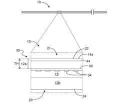
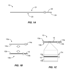
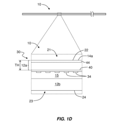
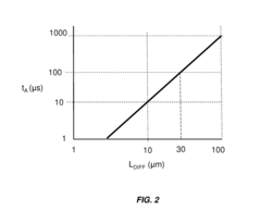
Laser annealing systems and methods with ultra-short dwell times
PatentActiveUS20160240407A9
Innovation
- The development of ultra-fast laser annealing systems using one or two laser beams that overlap, with a primary and secondary laser system, where the secondary laser scans the wafer surface at dwell times between 1 μs and 100 μs, achieving a peak annealing temperature between 350° C. and 1250° C. while maintaining temperature uniformity within ±3° C., utilizing a thermal emission detector and controller to adjust power and ensure consistent annealing.
Ultrafast laser annealing with reduced pattern density effects in integrated circuit fabrication
PatentInactiveUS8309474B1
Innovation
- The method involves using a dual-laser system where a first laser pre-heats the patterned surface to a non-melt temperature within 400°C of the melt temperature, and a second pulsed laser heats it up to the melt temperature, optimizing temperature uniformity by controlling the non-melt and melt laser beams' configurations and scanning patterns.
Material Compatibility and Process Parameters
Material compatibility is a critical factor in ultrafast laser annealing processes, as different materials respond uniquely to laser energy absorption and thermal diffusion. Silicon-based semiconductors remain the most extensively studied materials, exhibiting excellent compatibility with ultrafast laser annealing due to their well-characterized optical and thermal properties. Compound semiconductors such as GaAs and InP demonstrate varying degrees of compatibility, with challenges related to thermal decomposition and surface defect formation requiring precise parameter control.
Metal thin films present another category with distinct behavior patterns. Gold and copper films show high reflectivity at standard laser wavelengths, necessitating higher energy densities or wavelength optimization. Aluminum films, while more absorptive, face oxidation challenges that can compromise annealing quality. Refractory metals like tungsten and molybdenum exhibit superior thermal stability but require significantly higher energy densities to achieve effective annealing.
Process parameters constitute the fundamental control mechanisms for ultrafast laser annealing quality. Pulse duration, typically ranging from femtoseconds to picoseconds, determines the heat-affected zone depth and thermal gradient. Industry standards increasingly favor sub-picosecond pulses for nanoscale applications where minimal thermal diffusion is critical. Pulse energy density (fluence) standards vary by material, with silicon processes typically operating between 0.1-2.0 J/cm², while compound semiconductors often require lower fluences to prevent decomposition.
Repetition rate standards have evolved significantly, with current industrial systems operating between 100 kHz to 5 MHz for optimal throughput without thermal accumulation effects. Beam profile uniformity represents another crucial parameter, with top-tier systems now achieving better than ±3% uniformity across the processing area. Scanning speed and pattern optimization have become standardized based on material thermal properties, with serpentine patterns predominating for large-area processing.
Environmental conditions during processing have established clear standards, with vacuum levels of 10⁻⁶ torr becoming standard for sensitive materials. Alternatively, inert gas environments using 99.999% pure argon or nitrogen are accepted for less sensitive applications. Temperature control systems maintaining substrate temperatures within ±1°C across the processing area represent the current industry benchmark for high-precision annealing processes.
Safety Protocols and Quality Assurance Frameworks
The implementation of ultrafast laser annealing processes necessitates comprehensive safety protocols and quality assurance frameworks to mitigate risks and ensure consistent results. Current industry standards require multi-layered safety systems that address both personnel protection and equipment integrity. These typically include Class 4 laser safety measures with interlocked enclosures, automated beam shutters, and specialized personal protective equipment (PPE) designed specifically for ultrafast laser wavelengths and power densities.
Regulatory compliance forms the foundation of these protocols, with organizations such as ANSI Z136, IEC 60825, and OSHA providing standardized guidelines for laser safety. These standards are continuously evolving to address the unique challenges posed by ultrafast laser systems, particularly regarding the management of high peak powers and potential for non-linear optical effects that may bypass conventional safety measures.
Quality assurance frameworks for ultrafast laser annealing must incorporate real-time monitoring systems capable of detecting process deviations at nanosecond or picosecond timescales. Leading manufacturers have developed integrated process monitoring solutions that combine high-speed imaging, spectroscopic analysis, and thermal mapping to provide comprehensive process verification. These systems typically feature closed-loop feedback mechanisms that can adjust laser parameters in real-time to maintain process stability.
Documentation and traceability requirements have become increasingly stringent, with ISO 9001-based quality management systems being adapted specifically for ultrafast laser processing. These frameworks mandate detailed process parameter logging, material certification, and statistical process control methodologies to ensure reproducibility across production batches.
Risk assessment methodologies specific to ultrafast laser annealing have emerged, focusing on identifying potential failure modes related to beam delivery, temporal pulse characteristics, and material-specific responses. FMEA (Failure Mode and Effects Analysis) approaches tailored to ultrafast processes have been developed by industry leaders to systematically address these unique challenges.
Calibration and maintenance protocols represent another critical component of quality assurance frameworks. Regular verification of pulse duration, beam profile, and power stability is essential, with calibration intervals typically ranging from daily checks to comprehensive monthly validations depending on application criticality. Specialized measurement equipment such as autocorrelators, FROG (Frequency-Resolved Optical Gating) systems, and high-speed photodetectors are becoming standard requirements for facilities utilizing ultrafast laser annealing.
Training and certification programs for operators and maintenance personnel have also been standardized, with organizations like the Laser Institute of America offering specialized courses focused on ultrafast laser safety and quality management. These programs emphasize both theoretical understanding and practical demonstration of competence in managing the unique challenges associated with ultrafast laser processes.
Unlock deeper insights with Patsnap Eureka Quick Research — get a full tech report to explore trends and direct your research. Try now!
Generate Your Research Report Instantly with AI Agent
Supercharge your innovation with Patsnap Eureka AI Agent Platform!