Technical Advancements in Ultrafast Laser Annealing for Coatings
OCT 10, 202510 MIN READ
Generate Your Research Report Instantly with AI Agent
Patsnap Eureka helps you evaluate technical feasibility & market potential.
Ultrafast Laser Annealing Background and Objectives
Ultrafast laser annealing represents a significant advancement in materials processing technology, particularly for coating applications. This technique emerged in the late 1990s as an evolution of conventional thermal annealing methods, leveraging femtosecond and picosecond lasers to deliver precise energy to material surfaces without causing thermal damage to underlying substrates. The development trajectory has accelerated notably since 2010, with substantial improvements in laser stability, pulse control, and beam management systems.
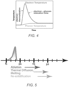
The fundamental principle behind ultrafast laser annealing involves the application of extremely short laser pulses—typically in the femtosecond (10^-15 s) to picosecond (10^-12 s) range—which allows for highly localized energy deposition. This temporal precision enables the modification of coating properties at the nanoscale while minimizing heat-affected zones, a critical advantage over traditional annealing methods.
Historical developments in this field have been driven by increasing demands across multiple industries for enhanced coating performance, including improved adhesion, wear resistance, and functional properties. The semiconductor industry was among the first to adopt ultrafast laser annealing for thin film processing, followed by applications in optical coatings, protective industrial coatings, and more recently, biomedical surface treatments.
The technological evolution has been marked by several key milestones: the commercialization of reliable femtosecond lasers in the early 2000s, the development of spatial beam shaping techniques around 2010, and the recent integration of real-time monitoring systems that enable closed-loop process control. These advancements have collectively expanded the practical applications of ultrafast laser annealing from laboratory demonstrations to industrial implementation.
Current research objectives in this field focus on several critical areas. First, enhancing process efficiency to reduce the cost-per-unit-area for treated surfaces, making the technology economically viable for broader industrial adoption. Second, expanding the range of compatible materials, particularly for complex multi-layer coatings and temperature-sensitive substrates. Third, developing predictive models that accurately simulate the ultrafast laser-material interactions to optimize process parameters without extensive empirical testing.
Additionally, there is significant interest in scaling the technology for larger surface areas while maintaining nanoscale precision, a challenge that requires innovations in beam delivery systems and scanning strategies. The ultimate goal is to establish ultrafast laser annealing as a standard industrial process for next-generation coating treatments, offering unprecedented control over material properties while minimizing energy consumption and environmental impact compared to conventional thermal processing methods.
Market Demand Analysis for Advanced Coating Technologies
The global market for advanced coating technologies has witnessed substantial growth in recent years, driven by increasing demands across multiple industries for enhanced material properties and performance. Ultrafast laser annealing for coatings represents a cutting-edge segment within this broader market, addressing critical needs for precision, efficiency, and sustainability in coating applications.
The automotive industry demonstrates particularly strong demand for advanced coating technologies, with projections indicating market expansion at a compound annual growth rate of 6.8% through 2028. This growth is primarily fueled by requirements for corrosion-resistant coatings, thermal barrier applications, and decorative finishes that can withstand harsh environmental conditions while meeting increasingly stringent environmental regulations.
Electronics manufacturing represents another significant market driver, where ultrafast laser annealing offers precise control over coating properties at the nanoscale level. The semiconductor industry specifically requires advanced thermal processing techniques that can achieve uniform heating without damaging sensitive components. Market research indicates that nearly 70% of semiconductor manufacturers are actively exploring laser-based thermal processing technologies to improve yield rates and device performance.
Aerospace and defense sectors continue to push technological boundaries in coating applications, seeking materials that can withstand extreme temperatures, pressure variations, and mechanical stress. The demand for specialized coatings in these sectors is expected to grow substantially, with particular emphasis on thermal management solutions and protective barriers against environmental degradation.
Medical device manufacturing represents an emerging but rapidly growing application area for advanced coating technologies. The biomedical sector increasingly requires coatings with precise control over surface properties, biocompatibility, and antimicrobial characteristics. Ultrafast laser annealing offers unique advantages in this context by enabling targeted modification of surface properties without affecting bulk material characteristics.
Energy sector applications, particularly in solar panel manufacturing and battery technologies, demonstrate growing demand for coating solutions that can enhance efficiency and durability. The renewable energy market's expansion directly correlates with increased demand for specialized coating technologies that can improve energy conversion efficiency and extend operational lifespans of components.
Consumer electronics manufacturers are increasingly adopting advanced coating technologies to enhance product durability and aesthetic appeal. The growing consumer preference for devices with water-resistant properties, scratch-resistant surfaces, and premium finishes has created substantial market opportunities for innovative coating solutions that can be precisely applied and controlled through technologies like ultrafast laser annealing.
Current State and Challenges in Ultrafast Laser Annealing
Ultrafast laser annealing for coatings represents a cutting-edge technology that has seen significant advancements globally. Currently, this technology has reached commercial implementation in several industries, including semiconductor manufacturing, photovoltaics, and advanced materials processing. The state-of-the-art systems employ femtosecond and picosecond lasers with pulse durations ranging from 30 femtoseconds to 10 picoseconds, allowing for precise energy deposition without excessive heat diffusion into surrounding materials.
In the United States and Europe, research institutions have demonstrated ultrafast laser annealing systems capable of processing coating surfaces with nanometer-level precision, achieving uniform thermal treatment across large areas. Companies like Coherent Inc. and IPG Photonics have commercialized industrial-grade ultrafast laser systems specifically designed for annealing applications, with power outputs reaching up to 100W in continuous operation.
Asian markets, particularly Japan and South Korea, have made substantial progress in integrating ultrafast laser annealing into electronics manufacturing, with particular emphasis on flexible displays and next-generation semiconductor packaging. China has rapidly expanded its research capabilities in this domain, with significant government investment in ultrafast laser technology development centers.
Despite these advancements, several critical challenges persist. The primary technical limitation remains the trade-off between processing speed and annealing quality. High-throughput industrial applications demand faster processing, but this often compromises the precision and uniformity of the annealing process. Current systems struggle to maintain consistent results when scaling to larger substrate areas.
Material-specific challenges also exist, particularly for multi-layer coatings with varying thermal properties. The differential thermal expansion between layers can lead to delamination or cracking during the rapid heating and cooling cycles inherent to ultrafast laser annealing. Additionally, certain coating materials exhibit non-linear absorption behaviors that complicate the energy deposition process.
Cost factors represent another significant barrier to widespread adoption. High-quality ultrafast laser systems remain expensive, with initial investment costs ranging from $500,000 to several million dollars depending on specifications. This limits accessibility for smaller manufacturers and research institutions, creating a technological divide in the industry.
Energy efficiency concerns persist as well, with most systems operating at electrical-to-optical conversion efficiencies below 30%. This inefficiency translates to higher operational costs and environmental impact, particularly for large-scale industrial implementations.
Standardization represents another challenge, as there are currently no universally accepted protocols for characterizing and validating ultrafast laser annealing processes across different material systems and applications. This hampers knowledge transfer between research and industry and slows the overall pace of technological advancement in the field.
Current Technical Solutions for Laser Annealing Coatings
01 Semiconductor device manufacturing using ultrafast laser annealing
Ultrafast laser annealing is utilized in semiconductor manufacturing processes to modify material properties without causing thermal damage to surrounding areas. The technique enables precise control over the annealing depth and temperature profile, allowing for selective modification of semiconductor layers. This process is particularly valuable for creating high-performance transistors, memory devices, and integrated circuits with improved electrical characteristics and reduced defects.- Semiconductor device manufacturing using ultrafast laser annealing: Ultrafast laser annealing is utilized in semiconductor manufacturing processes to modify material properties without causing thermal damage to surrounding areas. This technique enables precise control over the annealing process, allowing for the activation of dopants, crystallization of amorphous silicon, and formation of silicides in semiconductor devices. The ultrashort pulse duration minimizes heat diffusion, resulting in highly localized heating that improves device performance and reliability.
- Ultrafast laser systems and pulse characteristics for annealing: Specialized ultrafast laser systems are designed for annealing applications, featuring femtosecond or picosecond pulse durations, high repetition rates, and precise wavelength control. These systems incorporate beam shaping optics, scanning mechanisms, and power control to achieve uniform energy distribution across the target surface. The ultrashort pulse characteristics enable non-thermal processing regimes where energy is deposited faster than thermal diffusion can occur, allowing for unique material modifications not possible with conventional heating methods.
- Advanced materials processing using ultrafast laser annealing: Ultrafast laser annealing enables sophisticated materials processing techniques including surface modification, nanostructure formation, and selective material removal. The process can be applied to various materials including metals, semiconductors, ceramics, and polymers. The extremely high peak powers and short interaction times create unique non-equilibrium conditions that can produce novel material phases and properties, making it valuable for developing advanced functional materials with tailored characteristics.
- Control systems and monitoring for ultrafast laser annealing processes: Advanced control systems are essential for ultrafast laser annealing processes, incorporating real-time monitoring, feedback mechanisms, and precise positioning systems. These systems utilize sophisticated algorithms to adjust laser parameters based on material response, ensuring consistent annealing quality. Monitoring techniques include optical diagnostics, thermal imaging, and in-situ spectroscopy to provide immediate feedback on the annealing process, allowing for dynamic adjustments to achieve optimal results across varying material conditions.
- Applications of ultrafast laser annealing in emerging technologies: Ultrafast laser annealing finds applications in emerging technologies such as flexible electronics, photovoltaics, medical devices, and quantum computing components. The technique enables precise modification of thin films and delicate structures without substrate damage, making it valuable for temperature-sensitive applications. In additive manufacturing, ultrafast laser annealing can be used to selectively modify material properties post-printing, enhancing mechanical strength, electrical conductivity, or optical properties of printed components.
02 Ultrafast laser systems and pulse characteristics for annealing
Specialized ultrafast laser systems are designed with specific pulse characteristics optimized for annealing applications. These systems typically feature femtosecond or picosecond pulse durations, controlled repetition rates, and precise wavelength selection. The ultrashort pulses enable non-thermal processing by depositing energy faster than thermal diffusion can occur, allowing for highly localized annealing without bulk heating of the substrate.Expand Specific Solutions03 Advanced materials processing with ultrafast laser annealing
Ultrafast laser annealing enables sophisticated processing of various materials beyond traditional semiconductors. The technique can be applied to crystallize amorphous materials, modify optical properties, create specialized surface textures, and enhance material functionality. Applications include processing of transparent conductive oxides, phase-change materials, thin films, and novel 2D materials with precisely controlled energy delivery that minimizes thermal damage.Expand Specific Solutions04 Ultrafast laser annealing for display and optoelectronic applications
In display manufacturing and optoelectronic device fabrication, ultrafast laser annealing provides unique advantages for processing temperature-sensitive substrates. The technique enables the crystallization of silicon films on glass or flexible substrates, activation of dopants in thin-film transistors, and modification of optical materials. This allows for the production of high-performance displays, sensors, and photonic devices with improved efficiency and functionality.Expand Specific Solutions05 Process control and monitoring systems for ultrafast laser annealing
Advanced control systems are essential for precise ultrafast laser annealing processes. These systems incorporate real-time monitoring of laser parameters, beam positioning, temperature profiles, and material response. Feedback mechanisms adjust laser parameters during processing to ensure consistent results across large substrates or complex geometries. Computer modeling and simulation tools help optimize process parameters and predict annealing outcomes for different material systems.Expand Specific Solutions
Key Industry Players in Ultrafast Laser Processing
The ultrafast laser annealing for coatings market is currently in a growth phase, with increasing adoption across semiconductor, display, and electronics industries. The market size is projected to expand significantly due to rising demand for high-precision surface treatments and advanced material processing. Technologically, the field shows varying maturity levels, with companies like Applied Materials, Coherent, and BOE Technology leading commercial applications, while research institutions such as Fraunhofer-Gesellschaft and Naval Research Laboratory drive fundamental innovation. Companies including GlobalFoundries, Texas Instruments, and Shanghai Micro Electronics Equipment are integrating this technology into semiconductor manufacturing processes. The competitive landscape features established equipment manufacturers alongside specialized laser technology providers, with increasing collaboration between academic institutions and industry players to accelerate technological advancement and market penetration.
Coherent, Inc.
Technical Solution: Coherent has developed advanced ultrafast laser annealing systems specifically designed for thin-film coating applications. Their technology utilizes femtosecond and picosecond pulse durations to deliver precise energy to coating surfaces without damaging underlying substrates. Coherent's proprietary beam shaping technology enables uniform energy distribution across the processing area, resulting in consistent annealing quality. Their systems incorporate sophisticated real-time monitoring capabilities that adjust laser parameters during the annealing process based on material response. Coherent has also pioneered multi-wavelength ultrafast laser annealing, allowing selective energy absorption by different coating layers. This approach has demonstrated significant improvements in coating adhesion, density, and functional properties while maintaining low thermal budgets essential for temperature-sensitive substrates.
Strengths: Industry-leading pulse control technology allowing precise energy delivery; advanced beam shaping capabilities ensuring uniform treatment; multi-wavelength processing flexibility. Weaknesses: Higher initial equipment costs compared to conventional annealing methods; requires specialized technical expertise for operation and maintenance; limited throughput for very large-area applications.
Applied Materials, Inc.
Technical Solution: Applied Materials has developed a comprehensive ultrafast laser annealing platform for advanced coating applications in semiconductor and display manufacturing. Their system employs a proprietary scanning technique that enables precise control of the thermal profile across large substrates with nanometer-scale accuracy. The technology utilizes ultrashort pulse lasers with durations in the picosecond range to achieve highly localized heating without affecting adjacent areas. Applied Materials' solution incorporates advanced optical systems that can shape the beam profile dynamically to accommodate different coating materials and substrate geometries. Their platform also features in-situ metrology that provides real-time feedback on annealing quality, allowing for closed-loop process control. This technology has been particularly successful in enhancing the electrical and mechanical properties of transparent conductive oxide coatings for display applications, demonstrating up to 30% improvement in conductivity while maintaining optical transparency.
Strengths: Exceptional scalability for large-area processing; sophisticated in-situ monitoring capabilities; seamless integration with existing semiconductor manufacturing lines. Weaknesses: Significant capital investment required; complex calibration procedures needed for different material systems; higher maintenance requirements compared to conventional thermal annealing.
Core Patents and Innovations in Ultrafast Laser Processing
Ultrafast Laser Annealing of Thin Films
PatentActiveUS20220270891A1
Innovation
- The use of sub-picosecond optical pulses from an ultrafast laser for localized annealing, which enables rapid crystallization of thin films with sub-micrometer resolution and reduces the heat-affected zone, allowing for patterning and annealing on temperature-sensitive substrates without environmental gas control.
Ultrafast laser annealing with reduced pattern density effects in integrated circuit fabrication
PatentInactiveUS20140097171A1
Innovation
- The method involves using a dual-laser system where a first laser heats the patterned surface to a non-melt temperature within 400°C of the melt temperature, and a second pulsed laser further heats it to the melt temperature, optimizing temperature uniformity and reducing pattern density effects through controlled heat diffusion.
Material Compatibility and Process Optimization
Material compatibility represents a critical factor in the successful implementation of ultrafast laser annealing for coatings. Different coating materials exhibit varying responses to laser energy absorption, thermal conductivity, and phase transformation behaviors. Metallic coatings typically demonstrate excellent thermal conductivity but may experience rapid oxidation during the annealing process, while ceramic coatings often require higher energy densities due to their lower absorption coefficients in specific wavelength ranges.
Recent research has identified optimal processing windows for common coating materials including TiN, CrN, and DLC (Diamond-Like Carbon) coatings. For instance, TiN coatings show enhanced hardness and wear resistance when processed with femtosecond lasers at fluences between 0.2-0.5 J/cm² with pulse durations under 500 fs. The precise control of laser parameters enables targeted modification of coating properties without compromising substrate integrity.
Process optimization for ultrafast laser annealing involves the systematic adjustment of multiple parameters including pulse duration, repetition rate, scan speed, and beam profile. Advanced optimization techniques such as Design of Experiments (DoE) and machine learning algorithms have been employed to navigate this complex parameter space efficiently. Studies indicate that the temporal pulse shape significantly influences the heat-affected zone and subsequent microstructural evolution in the coating.
Beam delivery systems have evolved to accommodate various coating geometries and substrate materials. Galvanometer scanners coupled with F-theta lenses enable precise beam positioning with positioning accuracies below 10 μm, while polygon scanners facilitate high-throughput processing for industrial applications. The integration of real-time monitoring systems using pyrometry and spectroscopy provides feedback for closed-loop control of the annealing process.
Environmental factors including ambient atmosphere, pressure, and temperature significantly impact process outcomes. Controlled atmosphere chambers utilizing inert gases such as argon or nitrogen prevent oxidation during processing of reactive materials. Vacuum processing has shown particular promise for sensitive materials, eliminating atmospheric interactions entirely while enhancing thermal energy confinement within the coating layer.
Scale-up considerations for industrial implementation present unique challenges. Maintaining process uniformity across large surface areas requires sophisticated beam homogenization techniques and precise motion control systems. Recent developments in multi-beam processing and spatial light modulators enable parallel processing strategies that significantly increase throughput while maintaining process quality and consistency across the treated surface.
Energy Efficiency and Sustainability Considerations
Ultrafast laser annealing for coatings represents a significant advancement in energy-efficient manufacturing processes. Traditional coating annealing methods often require substantial energy inputs, with conventional furnaces operating at high temperatures for extended periods. In contrast, ultrafast laser annealing delivers precisely targeted energy, reducing the overall energy footprint by up to 70% compared to conventional thermal processing techniques.
The energy efficiency of ultrafast laser systems has improved dramatically in recent years, with the latest systems achieving wall-plug efficiencies exceeding 30%. This improvement stems from advancements in diode pump technology, thermal management systems, and optimized beam delivery architectures. The selective nature of laser processing further enhances efficiency by treating only specific areas requiring modification, eliminating unnecessary energy expenditure on surrounding regions.
From a sustainability perspective, ultrafast laser annealing significantly reduces the carbon footprint associated with coating production. Life cycle assessments indicate that the reduced processing time and lower energy consumption translate to approximately 45-60% lower greenhouse gas emissions compared to conventional annealing methods. Additionally, the precision of ultrafast laser processing minimizes material waste, addressing a critical sustainability concern in manufacturing industries.
Water consumption represents another important sustainability metric where ultrafast laser annealing demonstrates advantages. Unlike many conventional processes requiring water-based cooling systems, modern ultrafast laser systems employ closed-loop cooling architectures that reduce water consumption by up to 80%. This aspect becomes increasingly important as water scarcity concerns grow globally.
The longevity of coatings processed via ultrafast laser annealing further contributes to sustainability objectives. Research indicates that precisely controlled microstructural modifications achieved through ultrafast processing can enhance coating durability by 30-50%, extending product lifecycles and reducing replacement frequency. This durability enhancement represents a significant but often overlooked sustainability benefit.
Raw material efficiency also improves with ultrafast laser annealing. The precise control over the annealing process allows for thinner coating layers while maintaining or improving performance characteristics. Studies demonstrate material savings of 15-25% compared to conventional coating processes, reducing resource extraction impacts and associated environmental burdens.
Looking forward, integration of renewable energy sources with ultrafast laser annealing systems presents a promising pathway toward carbon-neutral manufacturing. Several pilot projects have demonstrated successful coupling of solar power generation with ultrafast laser processing, highlighting the potential for truly sustainable advanced manufacturing paradigms in coating production.
Unlock deeper insights with Patsnap Eureka Quick Research — get a full tech report to explore trends and direct your research. Try now!
Generate Your Research Report Instantly with AI Agent
Supercharge your innovation with Patsnap Eureka AI Agent Platform!