What Advances Ultrafast Laser Annealing Brings to Semiconductor Aging
OCT 10, 20259 MIN READ
Generate Your Research Report Instantly with AI Agent
Patsnap Eureka helps you evaluate technical feasibility & market potential.
Ultrafast Laser Annealing Background and Objectives
Ultrafast laser annealing (ULA) represents a significant technological advancement in semiconductor manufacturing, emerging from decades of thermal processing evolution. Initially developed in the early 2000s, this technology has progressed from experimental concepts to practical implementation in advanced semiconductor fabrication. The fundamental principle involves utilizing ultra-short laser pulses (typically in femtosecond to picosecond range) to deliver precise thermal energy to semiconductor materials, enabling controlled modification of material properties without excessive heat diffusion to surrounding areas.
The evolution of ULA technology has been driven by the semiconductor industry's relentless pursuit of Moore's Law and the increasing challenges of device miniaturization. Traditional annealing methods, including furnace annealing and rapid thermal processing (RTP), have reached their physical limitations in addressing the complex requirements of modern semiconductor devices, particularly in managing aging-related degradation mechanisms.
Recent advancements in ultrafast laser systems, including improved beam quality, higher repetition rates, and more precise spatial control, have significantly enhanced the capabilities of ULA technology. These improvements have enabled more effective management of semiconductor aging phenomena, including hot carrier injection, bias temperature instability, and electromigration, which have become increasingly problematic as device dimensions shrink below 10nm.
The primary technical objective of ULA in addressing semiconductor aging is to provide a highly controlled method for repairing lattice defects and restoring optimal electrical characteristics without compromising device integrity. This involves precise manipulation of thermal profiles at the nanoscale, enabling selective modification of material properties while maintaining the overall device structure and functionality.
Secondary objectives include extending device lifetime, improving reliability in extreme operating conditions, and enabling more aggressive design rules by mitigating aging-related performance degradation. Additionally, ULA aims to reduce the environmental impact of semiconductor manufacturing by minimizing the need for device replacement and extending the useful life of electronic components.
From a research perspective, ULA technology seeks to establish fundamental understanding of the interaction between ultrafast laser pulses and semiconductor materials, particularly focusing on the kinetics of defect formation and recovery. This knowledge is essential for developing predictive models and optimization strategies for industrial implementation.
The long-term technological goal is to integrate ULA as a standard process in semiconductor manufacturing and maintenance workflows, potentially enabling in-situ rejuvenation of aging devices in critical applications. This would represent a paradigm shift from the current approach of designing for inevitable degradation to implementing active management of device aging throughout the product lifecycle.
Semiconductor Industry Demand Analysis
The semiconductor industry faces unprecedented demand for advanced manufacturing processes that can address the critical issue of device aging. As Moore's Law continues to push transistor dimensions to their physical limits, reliability challenges have become increasingly prominent. Market analysis indicates that the global semiconductor industry, valued at approximately $573 billion in 2022, is projected to reach $1.38 trillion by 2029, with a significant portion of this growth driven by demands for more reliable and longer-lasting semiconductor devices.
Device aging phenomena, including hot carrier injection (HCI), bias temperature instability (BTI), and time-dependent dielectric breakdown (TDDB), have become major concerns as feature sizes shrink below 5nm. Industry reports suggest that addressing these reliability issues could potentially reduce warranty costs by 15-20% and extend device lifetimes by 30-40%, representing billions in value across the semiconductor ecosystem.
The automotive semiconductor segment, expected to grow at a CAGR of 14.5% through 2028, demonstrates particularly stringent reliability requirements, with vehicles now containing over 1,000 semiconductor chips per luxury vehicle. These components must withstand harsh operating conditions for 10-15 years, creating substantial demand for aging-resistant semiconductor technologies.
Data centers represent another critical market segment driving demand for aging-resistant semiconductors. With global data center investments reaching $227 billion in 2022, operators face significant challenges from semiconductor aging that impacts energy efficiency and system reliability. Industry studies indicate that aging-related performance degradation can increase data center power consumption by 5-8% annually.
Mobile device manufacturers are similarly affected by semiconductor aging issues, as consumers increasingly expect longer device lifespans. Market research shows that extending smartphone useful life by just one year through improved semiconductor reliability could reduce electronic waste by approximately 50 million devices annually.
The demand for ultrafast laser annealing solutions is further amplified by the industry's transition to new materials and 3D architectures. Gate-all-around (GAA) transistors, silicon carbide (SiC), and gallium nitride (GaN) technologies all require precise thermal processing that conventional rapid thermal annealing cannot adequately provide. Industry forecasts suggest that the market for specialized annealing equipment addressing these advanced node requirements will grow at 18% annually through 2027.
Current State and Challenges in Semiconductor Aging
Semiconductor aging remains a critical challenge in the microelectronics industry, affecting device reliability, performance, and longevity. Current semiconductor technologies face accelerated aging mechanisms due to continuous miniaturization and increasing operational demands. Hot carrier injection (HCI), bias temperature instability (BTI), time-dependent dielectric breakdown (TDDB), and electromigration represent the primary aging mechanisms that degrade semiconductor performance over time. These phenomena manifest as threshold voltage shifts, decreased carrier mobility, and increased leakage currents, ultimately leading to device failure.
The semiconductor industry currently employs various approaches to mitigate aging effects, including design-for-reliability techniques, redundancy implementation, and aging-aware circuit design. However, these methods often result in performance trade-offs or increased manufacturing costs. Traditional thermal annealing processes used to repair crystalline defects and reduce aging effects typically require high temperatures that can damage surrounding structures in advanced node technologies.
Ultrafast laser annealing (ULA) has emerged as a promising solution, offering precise, localized heating that minimizes thermal damage to adjacent structures. Current ULA implementations utilize femtosecond or picosecond lasers to deliver energy in extremely short pulses, enabling temperature control at the nanoscale. Despite its potential, ULA faces significant technical challenges including thermal management, process uniformity, and integration with existing semiconductor manufacturing workflows.
The geographical distribution of semiconductor aging research shows concentration in East Asia (particularly Taiwan, South Korea, and Japan), North America, and Europe. Leading research institutions like TSMC, Samsung, Intel, and imec are investing heavily in aging mitigation technologies, with ULA receiving increased attention in recent years.
A major technical constraint in current ULA applications is the difficulty in achieving uniform annealing across different semiconductor materials and structures. The varying optical and thermal properties of materials used in modern semiconductor devices create challenges in delivering consistent energy distribution. Additionally, the industry lacks standardized metrology tools for real-time monitoring of the ULA process, making quality control and process optimization difficult.
The economic factors also present significant challenges, as implementing ULA technology requires substantial capital investment in specialized equipment and process development. Smaller semiconductor manufacturers find these costs prohibitive, creating potential market concentration issues.
Regulatory and environmental considerations further complicate the landscape, with increasing pressure to reduce energy consumption and environmental impact of semiconductor manufacturing processes. While ULA potentially offers energy efficiency advantages over conventional annealing methods, comprehensive lifecycle assessments are still needed to validate these benefits across different application scenarios.
Current Ultrafast Laser Annealing Solutions
01 Ultrafast laser annealing techniques for semiconductor processing
Ultrafast laser annealing techniques employ femtosecond or picosecond lasers to precisely modify semiconductor properties. These techniques allow for controlled heating and cooling of semiconductor materials at extremely high speeds, enabling precise modification of crystal structures without causing thermal damage to surrounding areas. The ultrafast nature of the process helps in reducing defects and improving overall semiconductor performance while extending device lifespan.- Ultrafast laser annealing techniques for semiconductor processing: Ultrafast laser annealing techniques employ femtosecond or picosecond lasers to precisely modify semiconductor properties. These techniques enable controlled heating and cooling of semiconductor materials at extremely high rates, allowing for precise modification of crystal structures without excessive thermal diffusion. The ultrafast nature of the process helps in maintaining the integrity of surrounding structures while effectively annealing the target areas, making it suitable for advanced semiconductor manufacturing processes.
- Mitigating semiconductor aging effects through laser treatment: Laser annealing can be used to mitigate aging effects in semiconductor devices by repairing crystalline defects and reducing charge trapping. The process involves controlled energy delivery to semiconductor materials, which can heal lattice imperfections that develop over time due to operational stress. This treatment can restore electrical characteristics of aged semiconductors, extending device lifetime and maintaining performance parameters. The technique is particularly valuable for high-reliability applications where device degradation must be minimized.
- Pulse duration and energy control in laser annealing systems: Precise control of laser pulse duration and energy is critical in ultrafast laser annealing systems for semiconductor processing. By manipulating these parameters, manufacturers can achieve specific annealing effects while preventing damage to sensitive semiconductor structures. Advanced systems incorporate sophisticated feedback mechanisms to maintain consistent energy delivery across the treated surface. This control enables selective modification of semiconductor properties at nanoscale dimensions, allowing for targeted improvements in device performance and reliability.
- Integration of ultrafast laser annealing in semiconductor manufacturing: Integrating ultrafast laser annealing into semiconductor manufacturing workflows requires specialized equipment and process control systems. These systems must coordinate with existing fabrication steps while maintaining throughput requirements. The integration includes automated handling systems, precise positioning mechanisms, and quality control measures to ensure consistent results across wafers. Advanced manufacturing lines incorporate in-situ monitoring to verify annealing effectiveness and adjust parameters in real-time, enabling high-yield production of devices with enhanced reliability characteristics.
- Novel applications of ultrafast laser annealing for emerging semiconductor technologies: Ultrafast laser annealing enables novel applications in emerging semiconductor technologies, including flexible electronics, quantum computing components, and advanced memory devices. The technique allows for localized modification of material properties without affecting temperature-sensitive substrates or adjacent structures. Researchers are exploring applications in two-dimensional materials, wide-bandgap semiconductors, and heterogeneous integration platforms. These advanced applications leverage the unique capabilities of ultrafast lasers to achieve material transformations that would be impossible with conventional thermal processing methods.
02 Mitigating semiconductor aging through laser-induced defect repair
Laser annealing can be used to repair defects that accumulate in semiconductors over time due to aging processes. By applying ultrafast laser pulses to aged semiconductor materials, crystalline structures can be restored, and defects such as dislocations and vacancies can be eliminated. This process effectively rejuvenates semiconductor components, extending their operational lifetime and maintaining performance characteristics that would otherwise degrade with time.Expand Specific Solutions03 Pulse duration and energy optimization for semiconductor annealing
The effectiveness of ultrafast laser annealing in addressing semiconductor aging depends critically on optimizing laser pulse parameters. This includes precise control of pulse duration, energy density, repetition rate, and wavelength. Optimized parameters ensure that sufficient energy is delivered to repair defects and restructure crystalline formations without causing thermal damage or introducing new defects. Advanced control systems allow for real-time adjustment of these parameters based on material response.Expand Specific Solutions04 Integration of ultrafast laser annealing in semiconductor manufacturing
Incorporating ultrafast laser annealing into semiconductor manufacturing workflows requires specialized equipment and process integration. This includes automated systems for precise positioning, environmental controls to maintain optimal conditions during annealing, and integration with existing fabrication processes. These integrated systems can be used both in initial manufacturing and as part of maintenance procedures to address aging-related degradation in semiconductor components throughout their lifecycle.Expand Specific Solutions05 Novel materials and structures for laser-annealed semiconductors
Research into new semiconductor materials and structures specifically designed to benefit from ultrafast laser annealing processes shows promise for enhanced aging resistance. These include engineered substrates, doping profiles optimized for laser interaction, and multi-layer structures that facilitate controlled energy absorption. Such materials can be designed to respond more effectively to laser annealing treatments, resulting in more efficient defect repair and longer-lasting semiconductor components with improved resistance to aging-related performance degradation.Expand Specific Solutions
Key Players in Ultrafast Laser Annealing Market
Ultrafast laser annealing technology in semiconductor aging is currently in a growth phase, with the market expanding rapidly due to increasing demands for advanced semiconductor manufacturing processes. The global market size is projected to reach significant scale as semiconductor manufacturers seek more efficient aging solutions. Technologically, this field shows varying maturity levels across companies. Industry leaders like Taiwan Semiconductor Manufacturing Co., Samsung Electronics, and Tokyo Electron have made substantial advancements, while specialized players such as Gigaphoton, Veeco Instruments, and EO Technics are developing innovative solutions. Research institutions including Semiconductor Energy Laboratory and Kyushu University contribute fundamental research. The competitive landscape features both established semiconductor equipment manufacturers and emerging laser technology specialists, creating a dynamic environment for technological innovation and market development.
Gigaphoton, Inc.
Technical Solution: Gigaphoton has developed a specialized ultrafast laser annealing (ULA) platform specifically designed to address semiconductor aging challenges. Their system employs a hybrid approach combining femtosecond pulses (typically 100-300fs) with precisely controlled wavelength selection to target specific semiconductor materials and interfaces. The company's proprietary "Pulse-Shaped Annealing" technology enables dynamic control of the temporal profile of each laser pulse, allowing for unprecedented control over the thermal profile experienced by the semiconductor material. This approach enables selective modification of interface states and defect structures that contribute to aging phenomena without affecting critical device dimensions. Gigaphoton's system incorporates advanced beam homogenization technology that ensures uniform energy distribution across large areas, making it suitable for both wafer-level processing and packaged device treatment. Their research has demonstrated significant improvements in hot carrier degradation resistance and reduced bias temperature instability effects, particularly in power semiconductor applications where reliability under stress conditions is paramount.
Strengths: Exceptional control over thermal profiles through proprietary pulse shaping; demonstrated effectiveness in power semiconductor applications where aging effects are particularly challenging; compatible with both front-end and back-end processing. Weaknesses: System complexity requires specialized maintenance and calibration; higher cost per wafer compared to conventional annealing; process optimization can be time-consuming for new device architectures.
Veeco Instruments, Inc.
Technical Solution: Veeco Instruments has engineered an advanced ultrafast laser annealing (ULA) solution specifically targeting semiconductor aging mitigation. Their system utilizes a proprietary "Controlled Energy Deposition" approach that combines picosecond laser pulses with precise spatial and temporal control to address aging-related defects in semiconductor devices. The technology employs a wavelength-tunable laser source (typically operating in the 1030-1064nm range) that can be optimized for different semiconductor materials and device structures. Veeco's innovation lies in their multi-layer treatment methodology, which applies different pulse characteristics at various depths within the semiconductor stack, effectively addressing interface traps, oxide defects, and bulk material issues simultaneously. Their system incorporates advanced beam shaping optics that transform the Gaussian beam profile into a flat-top distribution, ensuring uniform treatment across the processed area. Veeco has demonstrated that their ULA process can reduce negative bias temperature instability (NBTI) degradation by up to 35% in advanced CMOS devices while simultaneously improving hot carrier injection (HCI) resistance, effectively extending device lifetime under operational stress conditions.
Strengths: Multi-layer treatment capability addresses aging mechanisms throughout the device stack; tunable wavelength allows optimization for different materials; demonstrated effectiveness against multiple aging mechanisms simultaneously. Weaknesses: Requires precise alignment and calibration for optimal results; higher initial investment compared to conventional annealing equipment; throughput limitations for high-volume manufacturing environments.
Core Innovations in Laser-Semiconductor Interaction
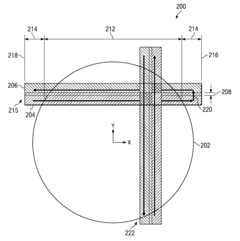
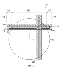
Laser annealing systems and methods with ultra-short dwell times
PatentActiveUS20160240407A9
Innovation
- The development of ultra-fast laser annealing systems using one or two laser beams that overlap, with a primary and secondary laser system, where the secondary laser scans the wafer surface at dwell times between 1 μs and 100 μs, achieving a peak annealing temperature between 350° C. and 1250° C. while maintaining temperature uniformity within ±3° C., utilizing a thermal emission detector and controller to adjust power and ensure consistent annealing.
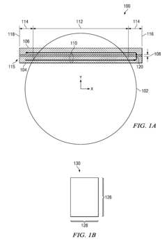
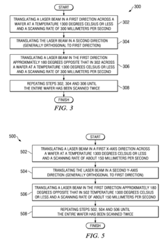
Methodology of improving the manufacturability of laser anneal
PatentActiveUS7932139B2
Innovation
- A method involving two successive laser annealing iterations with controlled temperature and scanning patterns, where the laser beam is scanned along the x-axis and then in a minus x-direction, and power is adjusted based on proximity to the workpiece edge to minimize thermal stress and warpage, optimizing the annealing process to reduce warpage and edge breakage.
Environmental Impact and Sustainability Considerations
Ultrafast laser annealing (ULA) technology represents a significant advancement in semiconductor manufacturing processes, offering not only performance improvements but also notable environmental benefits compared to traditional annealing methods. The environmental impact of semiconductor manufacturing has become increasingly scrutinized as the industry expands, making sustainability considerations essential for future technological developments.
ULA demonstrates superior energy efficiency compared to conventional thermal annealing processes. Traditional furnace-based annealing requires heating entire wafers for extended periods, consuming substantial energy. In contrast, ultrafast laser annealing delivers precise energy only to targeted areas for milliseconds or microseconds, resulting in energy consumption reductions of up to 40-60% depending on the specific application and implementation.
The localized nature of ULA processing significantly reduces the use of cooling water resources. Conventional annealing methods often require extensive cooling systems that consume large volumes of water, contributing to industrial water scarcity issues. ULA's precise energy delivery minimizes heat dissipation requirements, thereby reducing water consumption in cooling systems by approximately 30-50% compared to traditional methods.
Chemical usage represents another environmental advantage of ULA technology. The process requires fewer chemical treatments and cleaning steps than conventional annealing, reducing hazardous waste generation. Studies indicate that ULA implementation can decrease chemical consumption by 15-25% in semiconductor aging treatments, directly lowering the environmental footprint of manufacturing facilities.
From a lifecycle perspective, ULA contributes to extended semiconductor device lifespans. By more effectively addressing aging mechanisms like negative bias temperature instability (NBTI) and hot carrier injection (HCI), ULA-treated components demonstrate improved longevity. This extension of useful life reduces electronic waste generation, addressing a growing environmental concern in the electronics industry.
Carbon footprint reduction represents perhaps the most significant sustainability benefit of ULA technology. The combination of energy efficiency improvements, reduced resource consumption, and extended product lifespans contributes to lower greenhouse gas emissions across the semiconductor manufacturing chain. Early adopters of ULA technology have reported carbon footprint reductions of 20-35% for annealing processes compared to conventional methods.
As semiconductor manufacturers face increasing regulatory pressure and corporate sustainability targets, ULA technology offers a pathway to align technological advancement with environmental responsibility. The adoption of ULA for semiconductor aging treatment represents a rare win-win scenario where performance improvements coincide with reduced environmental impact, positioning this technology as a key contributor to more sustainable semiconductor manufacturing practices.
Integration with Advanced Packaging Technologies
The integration of ultrafast laser annealing (ULA) with advanced packaging technologies represents a significant frontier in semiconductor manufacturing innovation. As chipmakers continue to pursue heterogeneous integration and advanced packaging solutions like 2.5D and 3D integration, ULA offers unique capabilities that complement these packaging approaches. The low thermal budget and precise spatial control of ultrafast laser annealing make it particularly suitable for processing temperature-sensitive package structures without compromising their integrity.
In fan-out wafer-level packaging (FOWLP) and system-in-package (SiP) applications, ULA can selectively anneal specific regions while maintaining the structural integrity of adjacent areas. This capability is crucial when dealing with the complex multi-material interfaces present in advanced packages, where traditional thermal annealing methods might cause warpage, delamination, or thermal stress-induced failures.
For through-silicon via (TSV) technology, a cornerstone of 3D integration, ultrafast laser annealing offers potential solutions for stress management around vias and can improve the reliability of TSV structures by addressing defects at the silicon-metal interfaces. The non-contact nature of ULA also reduces the risk of mechanical damage to delicate 3D structures during the annealing process.
Chiplet-based architectures, which are gaining prominence in high-performance computing applications, benefit from ULA's ability to perform localized annealing at die-to-die interfaces. This can enhance the electrical performance and reliability of interconnects between chiplets, addressing one of the key challenges in heterogeneous integration.
Recent research demonstrates that ULA can be effectively applied to interposer technologies, where it helps optimize the electrical properties of redistribution layers (RDLs) without affecting the underlying silicon or embedded components. The millisecond to nanosecond processing times of ULA also align well with high-volume manufacturing requirements for advanced packaging.
From a reliability perspective, ULA treatment of critical interfaces in advanced packages has shown promising results in mitigating electromigration and stress migration concerns, which are particularly relevant for aging semiconductor devices in high-density packaging configurations. The precise control of the thermal profile during ULA allows for targeted reliability enhancement of specific failure-prone regions within a package.
As the semiconductor industry continues to push the boundaries of packaging density and performance, the integration of ULA into advanced packaging process flows represents a valuable approach to address both manufacturing challenges and long-term reliability concerns related to semiconductor aging in complex heterogeneous systems.
Unlock deeper insights with Patsnap Eureka Quick Research — get a full tech report to explore trends and direct your research. Try now!
Generate Your Research Report Instantly with AI Agent
Supercharge your innovation with Patsnap Eureka AI Agent Platform!