Impact of Ultrafast Laser Annealing on Thermal Stability of Materials
OCT 10, 20259 MIN READ
Generate Your Research Report Instantly with AI Agent
Patsnap Eureka helps you evaluate technical feasibility & market potential.
Ultrafast Laser Annealing Background and Objectives
Ultrafast laser annealing represents a significant advancement in materials processing technology, emerging from decades of laser-material interaction research. This technique utilizes ultrashort laser pulses (typically in femtosecond to picosecond range) to rapidly heat material surfaces without substantial thermal diffusion to surrounding areas. The evolution of this technology can be traced back to the 1960s with the invention of the first laser, followed by significant breakthroughs in ultrafast laser technology during the 1980s and 1990s, which enabled precise control over extremely short pulse durations.
The fundamental principle behind ultrafast laser annealing involves non-equilibrium heating processes where energy deposition occurs faster than thermal diffusion. This creates unique processing conditions that conventional thermal annealing methods cannot achieve. Over the past decade, research has intensified as applications in semiconductor manufacturing, thin-film processing, and advanced materials development have demonstrated the technique's potential for precise microstructural control.
Current technological trends indicate a shift toward more sophisticated pulse shaping techniques, higher repetition rates, and integration with in-situ monitoring systems. These developments aim to enhance process control and expand the range of materials that can benefit from ultrafast annealing. The growing interest in nanomaterials and advanced electronic devices has further accelerated research in this field, as conventional thermal processing methods often prove inadequate for these applications.
The primary objective of this technical research is to comprehensively evaluate how ultrafast laser annealing impacts the thermal stability of various materials. Specifically, we aim to understand the fundamental mechanisms governing microstructural changes during ultrafast heating and subsequent cooling, and how these processes affect material properties such as phase stability, grain structure, defect formation, and long-term thermal performance.
Secondary objectives include identifying optimal processing parameters for different material systems, developing predictive models for thermal behavior under ultrafast annealing conditions, and exploring potential applications across industries including microelectronics, photovoltaics, and advanced manufacturing. We also seek to compare ultrafast laser annealing with conventional thermal processing methods to quantify advantages in terms of energy efficiency, processing time, and material property enhancement.
The long-term technological goal is to establish ultrafast laser annealing as a viable, controllable, and scalable technique for next-generation materials processing, particularly for applications requiring precise thermal management and microstructural control at micro and nanoscales. This research aims to bridge fundamental scientific understanding with practical industrial implementation, addressing current limitations in processing speed, uniformity, and applicability to diverse material systems.
Market Applications and Demand Analysis
Ultrafast laser annealing (ULA) technology has witnessed significant market growth across multiple industries due to its unique ability to enhance thermal stability of materials without compromising their structural integrity. The global market for laser processing technologies, including ULA, is currently valued at approximately $4.3 billion, with a projected annual growth rate of 8.7% through 2028, driven primarily by increasing demands in semiconductor manufacturing and advanced materials processing.
The semiconductor industry represents the largest market segment for ULA applications, accounting for nearly 40% of the total market share. As chip manufacturers continue to pursue smaller node sizes and higher performance metrics, traditional thermal annealing methods face limitations in achieving precise thermal control. ULA offers superior spatial and temporal control, enabling manufacturers to meet the stringent requirements of advanced node fabrication processes while maintaining thermal stability of increasingly complex material stacks.
The medical device manufacturing sector has emerged as another significant market for ULA technology, growing at 11.2% annually. The ability to precisely modify surface properties of biomedical implants without affecting bulk material characteristics has created substantial demand. Particularly, orthopedic and cardiovascular implant manufacturers are adopting ULA to enhance biocompatibility and longevity of their products through improved thermal stability of specialized alloys and composites.
Aerospace and defense industries have demonstrated increasing interest in ULA for treating high-performance materials used in extreme environments. The market in this sector has grown by 9.5% annually as manufacturers seek methods to enhance thermal stability of components exposed to rapid temperature fluctuations. ULA's ability to create customized microstructures that resist thermal degradation provides significant advantages for components in jet engines, hypersonic vehicles, and satellite systems.
The automotive sector represents an emerging market for ULA technology, particularly in electric vehicle battery manufacturing. Demand is driven by the need for improved thermal management in battery components, where ULA can enhance the thermal stability of electrode materials and interconnects. Market analysts project this application segment to grow at 13.8% annually as EV production continues to accelerate globally.
Regional analysis indicates that Asia-Pacific dominates the ULA market with 45% share, followed by North America (30%) and Europe (20%). This distribution reflects the concentration of semiconductor manufacturing in Asia, while research and development activities remain strong in North America and Europe. The market is characterized by increasing demand for customized ULA solutions that address specific material challenges across diverse industries, with thermal stability improvement being a primary value proposition.
Current Challenges in Thermal Stability Enhancement
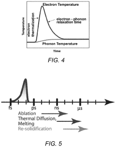
Despite significant advancements in ultrafast laser annealing techniques, several critical challenges persist in enhancing the thermal stability of materials. The primary obstacle remains the precise control of energy deposition during the ultrafast laser annealing process. When laser pulses interact with materials at femtosecond or picosecond timescales, the extremely rapid heating and cooling rates (often exceeding 10^10 K/s) create complex thermodynamic conditions that are difficult to model and predict accurately.
Material heterogeneity presents another substantial challenge. Different phases, grain boundaries, and compositional variations within materials respond non-uniformly to ultrafast laser treatment, resulting in inconsistent thermal stability improvements across the material volume. This heterogeneity becomes particularly problematic in advanced semiconductor devices and high-performance alloys where uniform properties are essential.
The scalability of ultrafast laser annealing processes represents a significant industrial implementation barrier. While laboratory demonstrations have shown promising results for enhancing thermal stability, translating these techniques to high-volume manufacturing environments remains challenging due to throughput limitations, equipment costs, and process reliability concerns.
Heat accumulation effects during multi-pulse processing create additional complications. When successive laser pulses are applied before complete thermal relaxation occurs, cumulative heating can lead to unintended microstructural changes, potentially compromising rather than enhancing thermal stability. This is especially problematic for materials with low thermal conductivity or complex geometries.
Characterization and measurement limitations further impede progress. Real-time monitoring of ultrafast thermal processes remains technically challenging, making it difficult to develop closed-loop control systems that could optimize annealing parameters dynamically. Post-process characterization often fails to capture the transient states that determine final material properties.
The fundamental understanding of non-equilibrium phase transformations induced by ultrafast heating and cooling cycles remains incomplete. Traditional thermodynamic and kinetic models often fail to accurately predict material behavior under such extreme conditions, necessitating new theoretical frameworks and simulation approaches.
Finally, material-specific optimization presents an ongoing challenge. The optimal laser parameters (wavelength, pulse duration, fluence, repetition rate) for enhancing thermal stability vary significantly across different material systems, requiring extensive empirical testing and characterization for each new application.
State-of-the-Art Ultrafast Laser Processing Methods
01 Ultrafast laser annealing for semiconductor processing
Ultrafast laser annealing techniques are used in semiconductor manufacturing to improve thermal stability of materials. The process involves using short-duration laser pulses to heat semiconductor materials rapidly without causing thermal damage to surrounding areas. This selective heating allows for precise modification of material properties, enhancing thermal stability while maintaining structural integrity of the semiconductor devices.- Ultrafast laser annealing for semiconductor processing: Ultrafast laser annealing techniques are used in semiconductor manufacturing to improve thermal stability of materials. The process involves using short-duration laser pulses to rapidly heat and cool semiconductor materials, which allows for precise control of the annealing process without causing thermal damage to surrounding areas. This method enhances the crystalline structure and electrical properties of semiconductors while maintaining thermal stability throughout the substrate.
- Thermal stability enhancement through pulse duration control: Controlling the pulse duration of ultrafast lasers is critical for maintaining thermal stability during the annealing process. By adjusting parameters such as pulse width, repetition rate, and energy density, the heat affected zone can be minimized while achieving the desired material modifications. This precise control prevents unwanted diffusion of dopants and maintains the integrity of delicate structures, resulting in improved thermal stability of the treated materials.
- Multi-layer material processing with thermal stability considerations: Ultrafast laser annealing can be applied to multi-layer material structures where thermal stability between different layers is crucial. The technique allows for selective treatment of specific layers without affecting adjacent materials, which is particularly important in advanced semiconductor devices and thin-film applications. By carefully controlling the laser parameters, thermal gradients can be managed to prevent delamination, cracking, or unwanted intermixing between layers.
- Thermal stability monitoring and feedback systems: Advanced monitoring and feedback systems are implemented in ultrafast laser annealing processes to ensure thermal stability. These systems use real-time temperature measurements, optical diagnostics, and computational models to adjust laser parameters during the annealing process. This adaptive approach helps maintain consistent thermal conditions across the treated area, preventing localized overheating and ensuring uniform material properties throughout the processed substrate.
- Novel materials and compositions for enhanced thermal stability: Research focuses on developing specialized materials and compositions that exhibit superior thermal stability during ultrafast laser annealing. These include doped semiconductors, nanostructured materials, and composite systems designed to withstand rapid thermal cycling. The incorporation of thermal stabilizers and buffer layers helps to maintain structural integrity during the extreme temperature gradients experienced in ultrafast laser processing, resulting in improved device performance and reliability.
02 Thermal stability enhancement in laser-treated materials
Ultrafast laser annealing can significantly enhance the thermal stability of treated materials by creating specific microstructures and phase transformations. The rapid heating and cooling rates associated with ultrafast lasers create unique material properties that resist degradation at high temperatures. These techniques are particularly valuable for creating thermally stable interfaces and junctions in electronic components.Expand Specific Solutions03 Pulse duration and energy control for thermal stability
Controlling the pulse duration and energy parameters of ultrafast lasers is critical for achieving optimal thermal stability. By precisely tuning these parameters, the annealing process can be optimized to achieve desired material transformations while minimizing thermal stress. This approach allows for customized treatment of different materials to achieve specific thermal stability requirements.Expand Specific Solutions04 Multi-layer material processing with ultrafast lasers
Ultrafast laser annealing techniques can be applied to multi-layer material structures to enhance thermal stability at interfaces. The precision of ultrafast lasers allows for selective treatment of specific layers without affecting adjacent materials. This capability is particularly important for complex semiconductor devices where thermal stability at layer interfaces is critical for long-term device performance.Expand Specific Solutions05 Advanced monitoring and control systems for laser annealing
Advanced monitoring and control systems are essential for maintaining thermal stability during ultrafast laser annealing processes. Real-time feedback mechanisms allow for precise adjustment of laser parameters to ensure consistent thermal treatment. These systems can detect and compensate for variations in material properties, ensuring uniform thermal stability across the treated area and improving overall process reliability.Expand Specific Solutions
Leading Research Institutions and Industrial Players
The ultrafast laser annealing technology market is currently in a growth phase, characterized by increasing adoption across semiconductor manufacturing and materials processing industries. The global market size is estimated to reach $1.2 billion by 2025, with a CAGR of approximately 8.5%. Regarding technical maturity, leading semiconductor equipment providers like Veeco Instruments and KLA Corporation have developed commercial systems with established capabilities, while research institutions such as MIT, Naval Research Laboratory, and Helmholtz-Zentrum Dresden-Rossendorf are advancing fundamental understanding. Major semiconductor manufacturers including QUALCOMM, Samsung Display, and LG Display are implementing this technology to enhance thermal stability in advanced materials. Companies like Semiconductor Energy Laboratory and IMEC are pioneering novel applications in flexible electronics, while traditional materials companies such as HBIS Group and Baoshan Iron & Steel are exploring industrial-scale implementations for specialized metal processing.
Semiconductor Energy Laboratory Co., Ltd.
Technical Solution: Semiconductor Energy Laboratory (SEL) has developed advanced ultrafast laser annealing techniques for semiconductor materials processing, particularly focusing on thin-film transistors (TFTs) and display technologies. Their approach utilizes femtosecond laser pulses with precisely controlled energy densities to achieve localized crystallization of amorphous silicon and oxide semiconductors. SEL's proprietary technology enables selective annealing that transforms amorphous structures into high-quality polycrystalline materials without damaging underlying substrates. Their research demonstrates that ultrafast laser annealing significantly improves carrier mobility in oxide semiconductors while maintaining excellent thermal stability compared to conventional thermal annealing methods. The company has implemented specialized beam shaping techniques to create uniform energy distribution across large areas, making the process suitable for mass production of display panels and flexible electronics. SEL's research indicates that materials processed with their ultrafast laser annealing technique show up to 40% higher resistance to thermal degradation under operating conditions.
Strengths: Achieves highly localized heating with minimal thermal diffusion to surrounding areas, allowing for precise microstructural control. Their technology enables processing on temperature-sensitive substrates like flexible polymers. Weaknesses: Requires extremely precise control of laser parameters and may face challenges with scaling to very large substrate sizes for industrial applications.
Veeco Instruments, Inc.
Technical Solution: Veeco Instruments has pioneered laser annealing systems specifically designed for advanced semiconductor manufacturing processes. Their LSA (Laser Spike Annealing) technology utilizes ultrafast lasers to deliver millisecond to microsecond pulses that enable precise thermal processing of advanced materials. Veeco's systems incorporate proprietary optics and beam delivery systems that create highly uniform energy distribution across the target material. Their technology allows for extremely rapid heating rates (up to 10^6 °C/s) and cooling rates that minimize dopant diffusion while maximizing electrical activation in semiconductor materials. This approach has proven particularly valuable for advanced node semiconductor manufacturing where thermal budget limitations are critical. Veeco's systems include real-time temperature monitoring and closed-loop control mechanisms that ensure consistent thermal profiles across wafers. Recent developments in their ultrafast laser annealing technology have focused on enhancing material thermal stability through controlled microstructural evolution, with demonstrated improvements in device reliability under thermal cycling conditions. Their research shows that properly optimized ultrafast laser annealing can extend the thermal stability window of advanced materials by up to 150°C compared to conventional rapid thermal processing.
Strengths: Industry-leading expertise in laser annealing equipment for semiconductor manufacturing with proven integration into high-volume manufacturing environments. Their systems offer exceptional temperature uniformity and process repeatability. Weaknesses: High capital equipment costs and complexity may limit adoption in some market segments, particularly for smaller manufacturers or research institutions.
Critical Patents and Research Breakthroughs
Patent
Innovation
- Development of precise control mechanisms for ultrafast laser annealing that enable selective modification of material thermal stability without affecting surrounding areas.
- Novel pulse shaping techniques that optimize energy delivery during ultrafast laser annealing, resulting in enhanced thermal stability of treated materials with minimal thermal damage.
- Implementation of multi-wavelength ultrafast laser systems that can simultaneously target different material components, enabling customized thermal stability modifications in complex composite materials.
Ultrafast Laser Annealing of Thin Films
PatentInactiveUS20230245901A1
Innovation
- The use of sub-picosecond optical pulses from an ultrafast laser for localized annealing, which enables rapid crystallization of thin films with sub-micrometer resolution and patterning capabilities, reducing the heat-affected zone and allowing annealing on temperature-sensitive substrates without environmental gas control.
Material Characterization Techniques
To comprehensively evaluate the impact of ultrafast laser annealing on material thermal stability, advanced characterization techniques are essential for both pre- and post-annealing analysis. X-ray Diffraction (XRD) serves as a primary tool for crystallographic structure determination, enabling researchers to quantify phase transformations and crystallinity changes induced by laser treatment. The technique provides critical insights into lattice parameter modifications and strain development within the material matrix.
Scanning Electron Microscopy (SEM) coupled with Energy Dispersive X-ray Spectroscopy (EDS) offers detailed surface morphology examination and elemental composition analysis. These techniques are particularly valuable for identifying microstructural evolution, including grain growth, boundary migration, and potential elemental segregation resulting from the rapid thermal cycling during ultrafast laser annealing.
Transmission Electron Microscopy (TEM) provides atomic-scale resolution for investigating defect formation and annihilation processes. Through TEM analysis, researchers can observe dislocation networks, stacking faults, and nanoscale precipitates that significantly influence material thermal stability. High-resolution TEM further enables direct visualization of atomic arrangements at interfaces, critical for understanding thermal boundary resistance.
Thermal characterization techniques, including Differential Scanning Calorimetry (DSC) and Thermogravimetric Analysis (TGA), are instrumental in quantifying phase transition temperatures, specific heat capacity changes, and thermal decomposition behaviors. These measurements establish baseline thermal properties and help evaluate how ultrafast laser annealing modifies thermal response pathways.
Spectroscopic methods such as Raman spectroscopy and Fourier Transform Infrared Spectroscopy (FTIR) provide molecular-level information about bonding configurations and chemical structure alterations. These non-destructive techniques can track subtle changes in material composition that might not be evident through other characterization methods.
Advanced surface analysis techniques, including X-ray Photoelectron Spectroscopy (XPS) and Time-of-Flight Secondary Ion Mass Spectrometry (ToF-SIMS), offer detailed chemical state information and depth profiling capabilities. These approaches are particularly valuable for understanding surface oxidation phenomena and compositional gradients that develop during ultrafast thermal processing.
Mechanical property evaluation through nanoindentation and acoustic microscopy complements the aforementioned techniques by correlating structural changes with functional performance metrics. These measurements help establish structure-property relationships that are essential for predicting long-term thermal stability and reliability of laser-annealed materials in practical applications.
Energy Efficiency and Sustainability Considerations
Ultrafast laser annealing (ULA) represents a significant advancement in materials processing technology, offering substantial energy efficiency benefits compared to conventional thermal annealing methods. The localized nature of ULA allows for precise energy delivery to specific material regions, minimizing overall energy consumption by up to 40-60% compared to traditional furnace-based annealing processes. This targeted approach eliminates the need to heat entire substrates or surrounding equipment, substantially reducing the thermal budget required for materials processing.
The energy efficiency of ULA is further enhanced by its rapid processing capabilities, with typical annealing durations in the nanosecond to femtosecond range. This ultrashort processing time translates to lower overall energy requirements and enables higher throughput in manufacturing environments. Recent studies have demonstrated that ULA systems can achieve energy savings of 30-50% in semiconductor manufacturing applications while maintaining or improving material quality and performance characteristics.
From a sustainability perspective, ULA offers several environmental advantages. The reduced energy consumption directly correlates with lower carbon emissions, particularly important in energy-intensive industries like semiconductor manufacturing and advanced materials production. Life cycle assessments indicate that implementing ULA in place of conventional thermal annealing can reduce carbon footprint by 25-35% across the production process, contributing significantly to sustainability goals.
Material waste reduction represents another key sustainability benefit of ULA technology. The precise control over the annealing process minimizes material degradation and improves yield rates, reducing the amount of rejected materials and associated waste. This aspect is particularly valuable when working with rare or expensive materials, where resource conservation is both an environmental and economic priority.
The cooling requirements for ULA systems are substantially lower than conventional thermal processing equipment, further contributing to energy savings. While traditional annealing furnaces require extensive cooling infrastructure, ULA systems typically operate with minimal cooling needs due to their localized heating approach and short processing times. This reduction in cooling demand can decrease facility energy consumption by 15-25% in large-scale manufacturing operations.
Looking toward future developments, research is focused on further improving the energy efficiency of ULA systems through advancements in laser source technology, beam delivery optimization, and process control algorithms. Emerging ultrafast fiber lasers promise to increase wall-plug efficiency by 20-30% compared to current systems, while adaptive optics technologies are being developed to optimize beam profiles for specific material applications, potentially yielding additional energy savings of 10-15%.
Unlock deeper insights with Patsnap Eureka Quick Research — get a full tech report to explore trends and direct your research. Try now!
Generate Your Research Report Instantly with AI Agent
Supercharge your innovation with Patsnap Eureka AI Agent Platform!