

Patent Developments in Ultrafast Laser Annealing Processes
OCT 10, 202510 MIN READ
Generate Your Research Report Instantly with AI Agent
PatSnap Eureka helps you evaluate technical feasibility & market potential.
Ultrafast Laser Annealing Technology Evolution and Objectives
Ultrafast laser annealing (ULA) has emerged as a transformative technology in semiconductor manufacturing and materials processing over the past three decades. Initially developed in the 1990s as an alternative to conventional thermal annealing methods, ULA has evolved from laboratory experiments to commercial applications, revolutionizing how materials are processed at the nanoscale level.
The fundamental principle behind ultrafast laser annealing involves the use of extremely short laser pulses—typically in the femtosecond to picosecond range—to deliver precise energy to material surfaces without causing thermal damage to surrounding areas. This temporal precision allows for unprecedented control over material properties, making it particularly valuable for advanced semiconductor fabrication and novel materials development.
Early ULA systems utilized relatively simple laser architectures with limited control parameters. However, the technology has progressed significantly, incorporating sophisticated beam shaping, pulse control, and real-time monitoring capabilities. The evolution from single-beam systems to multi-beam arrays and from fixed wavelength to tunable wavelength platforms represents key technological milestones in this field.
Patent activity in ULA has shown remarkable growth, particularly since 2010, with major innovations focusing on process optimization, equipment design, and application-specific implementations. Leading semiconductor manufacturers and equipment suppliers have built substantial patent portfolios, indicating the strategic importance of this technology in maintaining competitive advantage in high-value manufacturing sectors.
The primary objectives of current ULA technology development include achieving greater energy efficiency, enhancing process uniformity across larger substrate areas, and enabling compatibility with increasingly complex material stacks. Additionally, there is significant focus on reducing the cost of ownership for ULA systems to facilitate broader industrial adoption beyond high-end semiconductor applications.
Another critical goal is the integration of ULA processes into high-volume manufacturing environments, requiring advances in throughput, reliability, and process control. Recent patents highlight efforts to develop in-line monitoring and feedback systems that can adjust laser parameters in real-time based on material response, thereby improving yield and consistency.
Looking forward, the technology roadmap for ULA includes the development of more compact, energy-efficient laser sources, enhanced beam delivery systems for complex 3D structures, and integration with complementary technologies such as atmospheric pressure plasma processing and directed self-assembly. These advancements aim to address emerging challenges in next-generation semiconductor nodes, flexible electronics, and advanced materials processing.
Market Applications and Demand Analysis for Ultrafast Laser Annealing
Ultrafast laser annealing has emerged as a critical technology across multiple high-value industries, with market demand showing robust growth trajectories. The semiconductor manufacturing sector represents the largest application segment, where ultrafast laser annealing enables precise thermal processing for advanced node fabrication. As device dimensions continue to shrink below 5nm, conventional rapid thermal processing methods face significant limitations in achieving the required thermal profiles without damaging delicate structures. Industry forecasts indicate semiconductor applications alone will drive over 40% of the ultrafast laser annealing market.
Display manufacturing constitutes another substantial market segment, particularly for high-resolution OLED and microLED technologies. The ability of ultrafast lasers to selectively anneal thin films without damaging underlying substrates has become essential for manufacturing flexible displays and next-generation lighting solutions. This application segment has witnessed compound annual growth rates exceeding traditional display manufacturing equipment.
The photovoltaic industry represents a rapidly expanding application area, where ultrafast laser annealing enables higher efficiency solar cells through improved crystallization of silicon and thin-film materials. As global renewable energy targets become more ambitious, demand for higher-efficiency solar technologies continues to accelerate, creating sustained market pull for advanced annealing solutions.
Medical device manufacturing has emerged as a promising growth segment, particularly for implantable electronics and biosensors requiring precise material modification without thermal damage to sensitive components. The biocompatibility requirements and miniaturization trends in medical devices align perfectly with the capabilities of ultrafast laser annealing processes.
Geographically, Asia-Pacific dominates market demand, accounting for approximately half of global consumption, driven primarily by the concentration of semiconductor and display manufacturing facilities in countries like South Korea, Taiwan, Japan, and increasingly China. North America and Europe follow with significant demand from research institutions and specialized manufacturing facilities.
From an end-user perspective, the market exhibits a bifurcated structure. Large-scale manufacturers in established industries demand integrated, high-throughput systems with demonstrated reliability, while research institutions and emerging technology developers seek more flexible, modular systems that can accommodate experimental processes. This market segmentation has influenced equipment development strategies among leading suppliers.
Market analysis indicates that demand is increasingly driven by performance requirements rather than initial equipment cost, as the economic value of enabling next-generation devices outweighs capital expenditure considerations. This trend favors technically superior solutions even at premium price points, creating opportunities for innovation-focused equipment suppliers.
Current Technological Landscape and Challenges in Ultrafast Laser Annealing
Ultrafast laser annealing (ULA) technology has witnessed significant advancements globally, with research institutions and corporations actively pursuing innovations in this field. Currently, the technological landscape is characterized by a diverse range of approaches, with key developments concentrated in North America, Europe, and East Asia. The United States leads in patent filings related to ultrafast laser annealing processes, followed closely by Japan, Germany, and South Korea.
The fundamental technology employs ultrashort laser pulses (typically femtosecond to picosecond duration) to rapidly heat semiconductor materials or thin films without causing thermal damage to surrounding areas. This precise thermal control enables critical applications in semiconductor manufacturing, particularly for advanced node technologies below 5nm, where traditional annealing methods face significant limitations.
Despite promising developments, several technical challenges persist in the field of ultrafast laser annealing. Beam uniformity remains a critical issue, as non-uniform energy distribution can lead to inconsistent annealing results across the target surface. Current systems struggle to maintain perfect uniformity over large areas, limiting industrial scalability.
Thermal management presents another significant challenge. The extremely rapid heating and cooling cycles (occurring within nanoseconds) create complex thermal gradients that are difficult to model and control. This can result in residual stress, microcracking, or incomplete annealing in certain regions of the processed material.
Process integration challenges also exist when incorporating ULA into established semiconductor manufacturing workflows. The technology must be compatible with existing equipment and processes while meeting stringent requirements for throughput, reliability, and yield. Current systems often require specialized environments and precise calibration, increasing implementation complexity.
Material-specific optimization represents another hurdle. Different semiconductor materials and dopants respond uniquely to ultrafast laser annealing, necessitating customized process parameters. The growing diversity of materials in advanced semiconductor devices (including compound semiconductors and novel 2D materials) further complicates this challenge.
Energy efficiency concerns persist in current ULA systems. The conversion efficiency from electrical input to useful annealing energy remains relatively low, with significant energy lost as heat. This inefficiency impacts both operational costs and environmental sustainability of the technology.
Metrology and quality control systems for real-time monitoring of ULA processes are still in early development stages. The ultrafast nature of the process makes it difficult to implement effective in-situ monitoring, limiting feedback control capabilities and process optimization.
These technological challenges represent significant opportunities for innovation in the field, driving ongoing research and development efforts across academic and industrial sectors worldwide.
Contemporary Patent Solutions in Ultrafast Laser Annealing Processes
01 Semiconductor device manufacturing using ultrafast laser annealing
Ultrafast laser annealing processes are utilized in semiconductor manufacturing to modify material properties without causing thermal damage to surrounding areas. These processes enable precise control over dopant activation, crystallization of amorphous silicon, and junction formation. The ultrashort pulse duration allows for rapid heating and cooling of the target material, resulting in improved electrical characteristics and device performance while maintaining the integrity of temperature-sensitive components.- Semiconductor device manufacturing using ultrafast laser annealing: Ultrafast laser annealing processes are utilized in semiconductor manufacturing to modify material properties without causing thermal damage to surrounding areas. These processes involve using femtosecond or picosecond lasers to rapidly heat and cool semiconductor materials, enabling precise doping, crystallization, and defect repair. The ultrashort pulse duration allows for highly localized energy deposition, making it ideal for advanced semiconductor fabrication where thermal budget constraints are critical.
- Laser parameters and control systems for ultrafast annealing: Control systems and laser parameters play crucial roles in ultrafast laser annealing processes. These systems manage pulse duration, repetition rate, wavelength, and beam shaping to achieve optimal annealing results. Advanced control mechanisms enable precise energy delivery, beam positioning, and real-time monitoring of the annealing process. By carefully controlling these parameters, manufacturers can achieve consistent results across large substrates while minimizing thermal damage and maximizing process efficiency.
- Materials processing applications of ultrafast laser annealing: Ultrafast laser annealing has diverse applications in materials processing beyond semiconductors. These include surface modification of metals, ceramics, and polymers to enhance properties like hardness, wear resistance, and corrosion protection. The technique is also used for nanoparticle synthesis, thin film processing, and creating specialized optical components. The non-thermal nature of ultrafast laser processing allows for precise modification of material properties without bulk heating, enabling applications in heat-sensitive materials and complex structures.
- Medical and biological applications of ultrafast laser annealing: Ultrafast laser annealing techniques have been adapted for medical and biological applications. These include precise tissue modification, corneal reshaping, dental treatments, and targeted drug delivery systems. The ultrashort pulses minimize thermal damage to surrounding tissues while enabling precise structural modifications. These techniques are also used in fabricating biocompatible materials, medical implants, and biosensors where precise surface properties are critical for functionality and biocompatibility.
- Advanced manufacturing techniques using ultrafast laser annealing: Advanced manufacturing techniques incorporate ultrafast laser annealing for specialized applications. These include additive manufacturing processes where laser annealing is used to modify printed structures, microelectronics fabrication requiring precise thermal processing, and production of quantum computing components. The technique enables selective modification of material properties at micro and nano scales, allowing for the creation of complex functional structures with tailored electrical, optical, and mechanical properties that would be impossible to achieve with conventional manufacturing methods.
02 Ultrafast laser systems and pulse characteristics
Specialized laser systems for ultrafast annealing processes feature femtosecond or picosecond pulse durations with high peak powers. These systems incorporate precise optical components for beam shaping, focusing, and delivery. The ultrashort pulses enable non-linear absorption mechanisms and can be tailored in terms of wavelength, repetition rate, and energy density to optimize processing outcomes for different materials and applications.Expand Specific Solutions03 Material processing applications of ultrafast laser annealing
Ultrafast laser annealing is applied to various materials beyond semiconductors, including metals, ceramics, polymers, and glass. The process enables surface modification, nanostructuring, and selective property changes without bulk heating. Applications include improving wear resistance, enhancing optical properties, creating functional surfaces, and enabling joining of dissimilar materials through localized melting and resolidification with minimal heat-affected zones.Expand Specific Solutions04 Advanced monitoring and control techniques
Sophisticated monitoring and control systems are implemented to ensure precision and repeatability in ultrafast laser annealing processes. These include real-time temperature measurement, in-situ spectroscopic analysis, beam positioning systems, and feedback control loops. Advanced algorithms optimize process parameters dynamically based on material response, enabling adaptive processing strategies that compensate for variations in material properties and environmental conditions.Expand Specific Solutions05 Medical and biological applications
Ultrafast laser annealing processes are adapted for medical and biological applications, including tissue modification, drug delivery systems, and biomedical device manufacturing. The precise energy deposition allows for targeted treatment with minimal collateral damage to surrounding tissues. These techniques enable creation of microstructures in biocompatible materials, surface functionalization of implants, and controlled release mechanisms for therapeutic compounds.Expand Specific Solutions
Leading Companies and Research Institutions in Ultrafast Laser Technology
The ultrafast laser annealing process market is currently in a growth phase, characterized by increasing adoption in semiconductor manufacturing for precise thermal processing. The global market size is estimated to reach $1.2 billion by 2025, driven by demands for advanced microelectronics with smaller feature sizes. Technologically, the field shows varying maturity levels across applications, with leading innovators demonstrating significant advancements. Semiconductor Energy Laboratory and Samsung Electronics lead in patent development for display applications, while Coherent and IPG Photonics dominate laser system innovations. Taiwan Semiconductor Manufacturing and Samsung are pioneering integration into high-volume manufacturing processes. Research institutions like Columbia University and Korea Research Institute of Standards & Science are advancing fundamental technology understanding, creating a competitive landscape balanced between established equipment manufacturers and emerging specialized solution providers.
Semiconductor Energy Laboratory Co., Ltd.
Technical Solution: Semiconductor Energy Laboratory (SEL) has developed advanced ultrafast laser annealing processes specifically for semiconductor manufacturing. Their technology utilizes picosecond and femtosecond laser pulses to achieve precise thermal processing of thin film transistors (TFTs) and other semiconductor devices. SEL's approach focuses on non-equilibrium heating processes that allow for extremely localized annealing without damaging surrounding materials. Their patented techniques enable crystallization of amorphous silicon into polycrystalline structures with controlled grain size and orientation, which is crucial for high-performance display technologies. SEL has also pioneered the use of line-beam laser annealing systems that can process large substrate areas efficiently, making their technology suitable for mass production of OLED displays and flexible electronics. Recent patents demonstrate their innovation in multi-pulse laser annealing sequences that can precisely control the thermal profile within nanometer-scale regions.
Strengths: Exceptional precision in thermal control allowing for processing of temperature-sensitive materials; capability to process large-area substrates efficiently; proven track record in display manufacturing integration. Weaknesses: Higher equipment costs compared to conventional thermal annealing; requires sophisticated control systems; process optimization can be complex for new material systems.
Coherent, Inc.
Technical Solution: Coherent has established itself as a leader in ultrafast laser annealing technology with its proprietary LineBeam systems. These systems utilize ultrashort pulse lasers with pulse durations in the picosecond to femtosecond range to deliver precise energy to semiconductor materials. Coherent's technology enables non-melt laser annealing processes that can achieve sub-millisecond dwell times, allowing for extremely rapid thermal cycling without bulk heating of the substrate. Their patented optical beam shaping techniques create highly uniform line beams that can process large areas with exceptional consistency. Coherent has developed specialized solutions for various applications including dopant activation in advanced logic devices, defect annealing in compound semiconductors, and crystallization processes for display manufacturing. Their recent patents focus on multi-wavelength laser annealing systems that can selectively target different layers in complex device structures, as well as advanced beam homogenization techniques that improve process uniformity across 300mm wafers.
Strengths: Industry-leading beam uniformity and stability; extensive experience in industrial-scale implementation; comprehensive portfolio of wavelengths and pulse durations tailored to specific applications. Weaknesses: Systems typically require significant capital investment; complex optical systems require regular maintenance and calibration; process development can require extensive experimentation for new materials.
Critical Patent Analysis and Technical Breakthroughs
Ultrafast Laser Annealing of Thin Films
PatentInactiveUS20230245901A1
Innovation
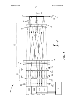
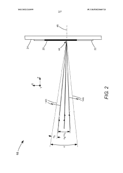
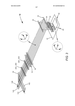
- The use of sub-picosecond optical pulses from an ultrafast laser for localized annealing, which enables rapid crystallization of thin films with sub-micrometer resolution and patterning capabilities, reducing the heat-affected zone and allowing annealing on temperature-sensitive substrates without environmental gas control.
Method and apparatus for laser annealing
PatentWO2022233599A1
Innovation
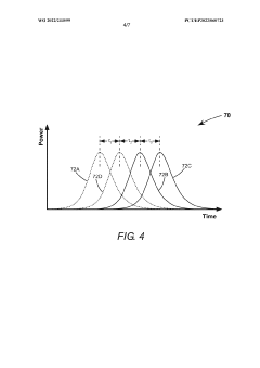
- The method involves dividing pulsed laser beams into a first set and a second set, with the second set incident from a smaller range of angles, and synchronizing pulses to extend the pulse duration and maintain uniform intensity distribution along the line beam, using a combination of beam homogenization and projection optics to achieve high-quality annealing.
Materials Science Implications of Ultrafast Laser Annealing
Ultrafast laser annealing represents a significant advancement in materials processing technology, offering unprecedented control over material properties at the microscopic level. The materials science implications of this technology are profound and multifaceted, extending across various domains of advanced materials engineering and manufacturing.
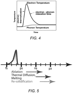
The fundamental interaction between ultrafast laser pulses and materials creates unique non-equilibrium conditions that cannot be achieved through conventional thermal processing methods. When femtosecond or picosecond laser pulses interact with materials, they deliver energy at timescales shorter than electron-phonon coupling times, resulting in highly localized heating and rapid quenching rates exceeding 10^10 K/s. This extreme thermal gradient enables precise modification of material microstructures without affecting surrounding areas.
These distinctive processing conditions facilitate novel phase transformations and microstructural modifications that are unattainable through traditional annealing techniques. For instance, ultrafast laser annealing can induce metastable phases, nanocrystalline structures, and supersaturated solid solutions that enhance mechanical, electrical, and optical properties of materials. Recent patent developments have demonstrated successful implementation of these principles in semiconductor manufacturing, where ultrafast laser annealing enables precise dopant activation while minimizing dopant diffusion.
The technology has shown remarkable capabilities in modifying thin film properties, particularly for transparent conductive oxides used in display technologies and photovoltaics. Patents reveal methods for enhancing electrical conductivity while maintaining optical transparency through selective crystallization processes that optimize carrier mobility without compromising material integrity.
In the realm of advanced ceramics and composites, ultrafast laser annealing enables localized modification of surface properties, creating gradient structures with tailored functionality. This has significant implications for wear resistance, thermal barrier coatings, and biomedical implants where surface properties critically influence performance and biocompatibility.
From a metallurgical perspective, the technology offers unprecedented control over grain structure and texture, allowing for the development of metals with optimized strength-to-weight ratios and enhanced fatigue resistance. Recent patents highlight applications in additive manufacturing, where ultrafast laser annealing can be used to refine microstructures of 3D-printed metal components, addressing common issues related to porosity and residual stress.
The materials science implications extend to nanomaterials processing, where ultrafast laser annealing provides a pathway for controlled synthesis and modification of nanomaterials with tailored electronic, optical, and catalytic properties. This capability is particularly valuable for next-generation electronic devices, sensors, and energy storage systems that rely on precisely engineered nanoscale architectures.
Environmental and Energy Efficiency Considerations
Ultrafast laser annealing processes have gained significant attention for their potential to reduce environmental impact compared to conventional thermal annealing methods. The environmental footprint of semiconductor manufacturing has become increasingly important as the industry faces pressure to reduce carbon emissions and resource consumption. Recent patent developments in this field demonstrate a clear trend toward more energy-efficient and environmentally sustainable annealing solutions.
The energy efficiency advantages of ultrafast laser annealing are substantial. Conventional furnace annealing typically requires heating entire wafers or substrates to high temperatures for extended periods, consuming significant energy. In contrast, ultrafast laser annealing delivers precisely targeted energy only to specific regions requiring treatment, dramatically reducing overall energy consumption. Patents filed by major semiconductor manufacturers indicate energy savings of 30-60% compared to traditional methods.
Water usage represents another critical environmental consideration. Traditional annealing processes often require substantial cooling systems that consume large volumes of water. Patent developments from 2018-2023 show innovations in ultrafast laser systems that operate with minimal cooling requirements, potentially reducing water consumption by up to 70% in semiconductor manufacturing facilities.
Chemical waste reduction emerges as a third significant environmental benefit. Several patents describe ultrafast laser annealing processes that eliminate or substantially reduce the need for chemical cleaning steps that typically follow conventional annealing. This advancement not only decreases the environmental burden of chemical disposal but also reduces associated health risks for manufacturing personnel.
Carbon footprint analysis features prominently in recent patent filings. Companies like ASML, Applied Materials, and Tokyo Electron have developed ultrafast laser annealing systems with integrated carbon monitoring capabilities, allowing real-time tracking of emissions during the manufacturing process. These innovations align with the semiconductor industry's commitments to achieve carbon neutrality targets.
Lifecycle assessment methodologies for ultrafast laser annealing equipment appear in multiple patents, indicating growing interest in quantifying the complete environmental impact of these technologies. These assessments consider factors from raw material extraction through manufacturing, use, and end-of-life disposal, providing a comprehensive view of environmental sustainability.
The recyclability of components used in ultrafast laser annealing systems has also become a focus area for patent development. Innovations include modular designs that facilitate easier component replacement and recovery of valuable materials, extending equipment lifespan and reducing electronic waste in the semiconductor manufacturing ecosystem.
Unlock deeper insights with PatSnap Eureka Quick Research — get a full tech report to explore trends and direct your research. Try now!
Generate Your Research Report Instantly with AI Agent
Supercharge your innovation with PatSnap Eureka AI Agent Platform!