The Application of Ultrafast Laser Annealing in Solar Cell Efficiency
OCT 10, 20259 MIN READ
Generate Your Research Report Instantly with AI Agent
Patsnap Eureka helps you evaluate technical feasibility & market potential.
Ultrafast Laser Annealing Technology Background and Objectives
Ultrafast laser annealing represents a significant advancement in solar cell manufacturing technology, emerging from decades of research in laser-material interactions. This technique utilizes ultra-short laser pulses, typically in the femtosecond to picosecond range, to selectively heat and modify semiconductor materials without causing thermal damage to surrounding areas. The evolution of this technology can be traced back to the early 2000s when ultrafast lasers began transitioning from laboratory curiosities to practical industrial tools.
The fundamental principle behind ultrafast laser annealing involves non-equilibrium heating processes that occur when materials absorb energy from extremely short laser pulses. Unlike conventional thermal annealing methods that require minutes or hours of processing time, ultrafast laser annealing can be completed in milliseconds or less, significantly reducing manufacturing time and energy consumption.
Recent technological advancements have enabled precise control over laser parameters such as pulse duration, repetition rate, and spatial beam profile, allowing for unprecedented customization of the annealing process. This has opened new possibilities for enhancing solar cell efficiency through targeted modification of material properties at the nanoscale level.
The primary objective of implementing ultrafast laser annealing in solar cell production is to overcome the efficiency limitations of current manufacturing techniques. Specifically, this technology aims to improve carrier lifetime, reduce surface recombination, and enhance dopant activation while minimizing thermal budget and processing time. These improvements directly translate to higher conversion efficiencies in the final solar cell products.
Another critical goal is to develop scalable processes that can be integrated into existing production lines without requiring complete retooling of manufacturing facilities. This includes designing laser systems capable of high-throughput processing compatible with industry-standard wafer sizes and handling equipment.
From a sustainability perspective, ultrafast laser annealing targets significant reductions in energy consumption during the manufacturing process. Conventional annealing methods often require heating entire wafers or panels to high temperatures for extended periods, whereas laser-based approaches can selectively process only the regions that require modification.
Looking forward, the technology roadmap for ultrafast laser annealing includes achieving sub-5% efficiency improvements in commercial solar cells within the next three years, with aspirations to push beyond the theoretical limits of current cell architectures through novel material modifications that are only possible with ultrafast processing techniques.
Solar Cell Market Demand Analysis
The global solar energy market has witnessed substantial growth over the past decade, driven by increasing environmental concerns, government incentives, and declining costs of solar technology. As of 2023, the global solar PV market was valued at approximately $197 billion, with projections indicating a compound annual growth rate (CAGR) of 13.8% through 2030. This growth trajectory underscores the significant market potential for advanced solar cell technologies, particularly those that enhance efficiency.
Efficiency improvements represent the most critical factor driving solar cell market demand. Current commercial silicon-based solar cells typically operate at 18-22% efficiency, while high-end models reach 24-25%. The market demonstrates a clear premium pricing structure for higher efficiency panels, with each percentage point improvement in efficiency commanding approximately 7-10% price premium. This efficiency-price relationship creates substantial market incentives for technologies like ultrafast laser annealing that promise efficiency enhancements.
Manufacturing cost reduction represents another crucial market driver. The solar industry operates on thin margins, with intense price competition from large-scale manufacturers. Technologies that can improve efficiency without significantly increasing production costs are highly sought after. Ultrafast laser annealing shows particular promise in this regard, as it can potentially be integrated into existing manufacturing lines with relatively modest capital investment compared to alternative efficiency-enhancing technologies.
Residential solar installations have emerged as a particularly promising market segment, growing at 15% annually in developed markets. This segment places higher value on efficiency due to limited installation space, making it an ideal target market for ultrafast laser annealing technology. Commercial and utility-scale installations, while more price-sensitive, still represent substantial market opportunities, especially as grid parity is achieved in more regions globally.
Geographically, China dominates global solar manufacturing, producing over 70% of global solar panels. However, recent policy shifts in the United States, European Union, and India aim to reduce dependence on Chinese solar imports, creating new market opportunities for advanced manufacturing technologies in these regions. The Inflation Reduction Act in the US alone allocates $369 billion toward clean energy initiatives, with significant portions directed toward solar manufacturing and deployment.
Emerging markets in Southeast Asia, Latin America, and Africa represent the fastest-growing demand centers for solar technology, with annual growth rates exceeding 20% in several countries. These markets are increasingly seeking higher efficiency solutions as they build out new energy infrastructure, creating additional demand for advanced solar cell technologies.
Current Status and Challenges in Laser Annealing for PV
Laser annealing technology has emerged as a promising approach for enhancing photovoltaic (PV) cell efficiency. Currently, the global landscape shows significant advancements in both continuous wave and pulsed laser annealing techniques, with ultrafast laser annealing gaining particular attention for its precision and reduced thermal impact. Research institutions across Europe, North America, and East Asia have established robust R&D programs, with notable progress in nanosecond and picosecond laser applications for silicon and thin-film solar cells.
The current technological maturity varies significantly across different laser annealing methods. Nanosecond laser annealing has reached industrial implementation in certain manufacturing processes, while ultrafast (femtosecond) laser annealing remains predominantly in the laboratory research phase. Mid-range technologies such as picosecond laser annealing are transitioning from advanced research to early commercialization, with several pilot production lines being established by leading PV manufacturers.
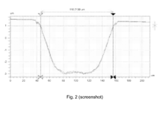
Despite promising developments, several critical challenges impede widespread adoption of laser annealing in PV manufacturing. The foremost technical barrier is achieving uniform thermal distribution across large-area substrates, particularly for next-generation large-format solar cells. Non-uniform annealing can create localized defects and inconsistent crystallization, ultimately reducing overall cell efficiency and increasing performance variability between cells.
Cost considerations present another significant hurdle. High-powered ultrafast laser systems require substantial capital investment, with current estimates suggesting a 30-50% higher initial equipment cost compared to conventional thermal annealing methods. The economic viability is further complicated by maintenance requirements and specialized operator training, creating barriers for smaller manufacturers and emerging markets.
Process integration challenges also persist, particularly in adapting existing production lines to incorporate laser annealing steps. The technology must be compatible with upstream and downstream processes without introducing contamination or creating bottlenecks in throughput. Current manufacturing lines optimized for conventional thermal processing require significant reconfiguration to accommodate laser-based processes.
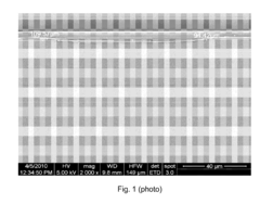
Material-specific challenges vary across different PV technologies. For crystalline silicon cells, laser-induced damage and incomplete dopant activation remain problematic. In thin-film technologies, precise control of phase transformations and interface properties during ultrafast annealing presents ongoing research challenges. Perovskite solar cells, while showing promise with laser processing, face stability issues when subjected to intense, localized heating.
Scaling limitations represent another significant constraint. Laboratory demonstrations have shown impressive results on small samples, but maintaining process control and uniformity at industrial scales (>1m²) remains technically demanding. Current laser scanning strategies struggle to balance throughput requirements with annealing quality at production scales.
The current technological maturity varies significantly across different laser annealing methods. Nanosecond laser annealing has reached industrial implementation in certain manufacturing processes, while ultrafast (femtosecond) laser annealing remains predominantly in the laboratory research phase. Mid-range technologies such as picosecond laser annealing are transitioning from advanced research to early commercialization, with several pilot production lines being established by leading PV manufacturers.
Despite promising developments, several critical challenges impede widespread adoption of laser annealing in PV manufacturing. The foremost technical barrier is achieving uniform thermal distribution across large-area substrates, particularly for next-generation large-format solar cells. Non-uniform annealing can create localized defects and inconsistent crystallization, ultimately reducing overall cell efficiency and increasing performance variability between cells.
Cost considerations present another significant hurdle. High-powered ultrafast laser systems require substantial capital investment, with current estimates suggesting a 30-50% higher initial equipment cost compared to conventional thermal annealing methods. The economic viability is further complicated by maintenance requirements and specialized operator training, creating barriers for smaller manufacturers and emerging markets.
Process integration challenges also persist, particularly in adapting existing production lines to incorporate laser annealing steps. The technology must be compatible with upstream and downstream processes without introducing contamination or creating bottlenecks in throughput. Current manufacturing lines optimized for conventional thermal processing require significant reconfiguration to accommodate laser-based processes.
Material-specific challenges vary across different PV technologies. For crystalline silicon cells, laser-induced damage and incomplete dopant activation remain problematic. In thin-film technologies, precise control of phase transformations and interface properties during ultrafast annealing presents ongoing research challenges. Perovskite solar cells, while showing promise with laser processing, face stability issues when subjected to intense, localized heating.
Scaling limitations represent another significant constraint. Laboratory demonstrations have shown impressive results on small samples, but maintaining process control and uniformity at industrial scales (>1m²) remains technically demanding. Current laser scanning strategies struggle to balance throughput requirements with annealing quality at production scales.
Current Ultrafast Laser Annealing Implementation Methods
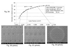
01 Pulse duration and energy optimization for laser annealing
Optimizing pulse duration and energy parameters is crucial for enhancing ultrafast laser annealing efficiency. By controlling the pulse width in the femtosecond to picosecond range and adjusting the energy density, heat distribution can be precisely managed to achieve desired material modifications while minimizing thermal damage to surrounding areas. This approach allows for more efficient energy transfer to the target material, resulting in improved annealing quality and processing speed.- Ultrafast laser annealing for semiconductor processing: Ultrafast laser annealing techniques are employed in semiconductor manufacturing to improve processing efficiency. These methods use short-duration laser pulses to precisely heat semiconductor materials, enabling controlled modification of material properties without excessive thermal diffusion. This approach allows for selective annealing of specific regions, improving dopant activation, reducing defects, and enhancing overall device performance while minimizing damage to surrounding areas.
- Pulse characteristics optimization for annealing efficiency: The efficiency of ultrafast laser annealing processes can be significantly improved by optimizing laser pulse characteristics. Parameters such as pulse duration, repetition rate, energy density, and wavelength are carefully controlled to achieve optimal annealing results. Advanced pulse shaping techniques and temporal control mechanisms help maximize energy transfer to the target material while minimizing unwanted thermal effects, resulting in more efficient and precise annealing processes.
- Material-specific annealing techniques: Different materials require specialized ultrafast laser annealing approaches to achieve maximum efficiency. Researchers have developed material-specific protocols that account for unique thermal, optical, and structural properties of various substrates including silicon, compound semiconductors, metals, and novel 2D materials. These tailored approaches optimize energy absorption, heat distribution, and phase transformation processes, resulting in more efficient annealing outcomes for specific material systems.
- Beam delivery and scanning strategies: Advanced beam delivery and scanning strategies significantly impact the efficiency of ultrafast laser annealing processes. Techniques such as beam shaping, homogenization, multi-beam processing, and sophisticated scanning patterns help distribute laser energy more uniformly across the target surface. These approaches minimize processing time, reduce energy consumption, and ensure consistent annealing results across large areas, thereby improving overall process efficiency and throughput.
- Real-time monitoring and feedback control systems: Integration of real-time monitoring and feedback control systems enhances ultrafast laser annealing efficiency. Advanced sensors and diagnostic tools continuously monitor process parameters such as temperature, reflectivity, and surface morphology during annealing. This data feeds into sophisticated control algorithms that dynamically adjust laser parameters to maintain optimal processing conditions. Such closed-loop systems improve process consistency, reduce energy waste, and enable adaptive processing for maximum annealing efficiency across varying material conditions.
02 Semiconductor processing applications
Ultrafast laser annealing provides significant efficiency improvements in semiconductor processing applications. The technique enables precise dopant activation, crystallization of amorphous silicon, and defect repair in semiconductor materials. The ultrashort pulses allow for localized heating without affecting adjacent structures, making it particularly valuable for advanced node semiconductor manufacturing where thermal budgets are tightly constrained and feature sizes are extremely small.Expand Specific Solutions03 Multi-beam and scanning techniques
Efficiency in ultrafast laser annealing can be enhanced through multi-beam approaches and advanced scanning techniques. By splitting a single high-power laser into multiple beams or employing sophisticated beam steering methods, larger areas can be processed simultaneously. These techniques improve throughput while maintaining the precision benefits of ultrafast lasers. Spatial light modulators and galvanometer scanners enable customized beam patterns that can be optimized for specific material requirements.Expand Specific Solutions04 Material-specific annealing optimization
Different materials require specific ultrafast laser annealing parameters to achieve optimal efficiency. For metals, semiconductors, ceramics, and polymers, the absorption characteristics, thermal conductivity, and phase transformation dynamics vary significantly. By tailoring the laser wavelength, pulse energy, and repetition rate to match the specific material properties, annealing efficiency can be substantially improved. This approach enables precise control over microstructure development and material properties.Expand Specific Solutions05 Feedback control systems for process monitoring
Implementing real-time feedback control systems significantly enhances ultrafast laser annealing efficiency. These systems monitor key process parameters such as surface temperature, reflectivity changes, and plasma formation during annealing. The collected data is used to dynamically adjust laser parameters, ensuring consistent results despite variations in material properties or environmental conditions. Advanced algorithms can predict optimal processing conditions, reducing waste and improving overall energy efficiency of the annealing process.Expand Specific Solutions
Key Industry Players in Ultrafast Laser and Solar Technologies
The ultrafast laser annealing market for solar cell efficiency is in a growth phase, with increasing adoption driven by demands for higher photovoltaic performance. Major players include established semiconductor equipment manufacturers like Coherent, Inc. and Lam Research Corp., alongside solar specialists such as JinkoSolar, Trina Solar, and Longi Solar. The technology is approaching commercial maturity, with research institutions (CEA, University of Florida) collaborating with industry leaders. Companies like SiOnyx and Intermolecular are advancing novel materials processing techniques, while traditional electronics giants Sony and Toshiba contribute specialized expertise. The competitive landscape features both vertically integrated solar manufacturers and specialized equipment providers, with innovation focused on improving cell efficiency while reducing production costs.
Zhejiang Jinko Solar Co. Ltd.
Technical Solution: Jinko Solar has implemented ultrafast laser annealing in their advanced n-type TOPCon solar cell production lines. Their proprietary approach combines ultrafast laser processing with specialized passivation techniques to achieve record-breaking cell efficiencies. The company utilizes picosecond lasers with precisely controlled pulse widths to selectively anneal the tunnel oxide and polysilicon layers in their TOPCon cells, creating optimal interface properties while minimizing bulk defects. This selective heating approach allows for improved carrier transport across critical junctions while maintaining the integrity of temperature-sensitive materials. Jinko's process incorporates multi-pass scanning algorithms that ensure uniform treatment across large-area cells, addressing one of the key challenges in scaling ultrafast laser annealing to commercial production. Their R&D team has demonstrated that this technique reduces contact resistance and enhances carrier selectivity, contributing to their achievement of cell efficiencies exceeding 25% in mass production. The company has successfully integrated this technology into their gigawatt-scale manufacturing facilities.
Strengths: Vertical integration allows for optimized process development specific to their cell architecture; demonstrated mass production capability; proven efficiency gains in commercial products. Weaknesses: Technology is specifically optimized for their proprietary cell designs; high implementation costs limit deployment across all production lines.
Maxeon Solar Pte Ltd.
Technical Solution: Maxeon Solar has pioneered the application of ultrafast laser annealing in their premium high-efficiency back-contact solar cells. Their proprietary approach utilizes femtosecond laser pulses to selectively modify the silicon surface properties without introducing thermal damage to the bulk material. This enables the creation of optimized local contact structures with minimal carrier recombination. Maxeon's technology incorporates a multi-wavelength laser processing system that can simultaneously address different layers of their complex cell architecture, including selective doping enhancement and contact formation. Their process achieves precise spatial control down to the micron level, allowing for optimized contact geometry that maximizes light absorption while minimizing electrical losses. The company has demonstrated that ultrafast laser annealing significantly improves the fill factor of their IBC (Interdigitated Back Contact) cells by reducing contact resistance while maintaining excellent passivation quality. This technology has been instrumental in Maxeon achieving cell efficiencies exceeding 25% in commercial production. Their latest generation process incorporates adaptive feedback systems that monitor the laser-material interaction in real-time, ensuring consistent results across production batches.
Strengths: Industry-leading efficiency in commercial cells; proprietary cell architecture optimized for laser processing; excellent long-term reliability of laser-processed cells. Weaknesses: Premium positioning limits market penetration; highly specialized equipment requirements increase manufacturing complexity.
Critical Patents and Research in Ultrafast Laser Annealing
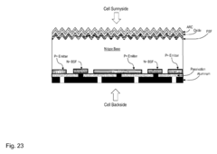
Laser annealing applications in high-efficiency solar cells
PatentInactiveEP2819181A1
Innovation
- The development of pulsed laser processing schemes with shorter pulse lengths, such as picoseconds and femtoseconds, and specific wavelengths like UV and IR, to minimize substrate damage during silicon and oxide ablation, allowing for selective ablation and doping without the need for wet cleaning, and the use of flat top laser beams for reduced damage and improved throughput.
Laser annealing applications in high-efficiency solar cells
PatentInactiveUS20130164883A1
Innovation
- The development of pulsed laser processing schemes with picoseconds or femtoseconds pulse lengths and specific wavelengths (UV, green, or IR) to minimize substrate damage, combined with advanced ablation techniques for selective doping, metal patterning, and passivation, allowing for precise control over contact areas and reduced recombination losses.
Cost-Benefit Analysis of Ultrafast Laser Integration
Integrating ultrafast laser annealing technology into solar cell manufacturing processes presents a complex economic equation that requires thorough analysis. Initial capital expenditure for ultrafast laser systems ranges from $500,000 to $2 million depending on power specifications, beam quality requirements, and automation capabilities. This represents a significant investment compared to conventional thermal annealing equipment, which typically costs 40-60% less.
Operational expenses must also be carefully considered. Ultrafast laser systems consume substantial electricity—approximately 10-15 kW for industrial-grade systems—contributing to ongoing costs. Maintenance requirements include regular replacement of optical components (every 6-12 months) and laser gain media (every 2-3 years), adding approximately 5-8% of the initial system cost annually to the operational budget.
However, these costs must be weighed against measurable efficiency improvements. Research demonstrates that ultrafast laser annealing can enhance solar cell conversion efficiency by 1.5-2.5 percentage points compared to conventional methods. For a production line manufacturing 100 MW of solar panels annually, this efficiency gain translates to approximately $3-5 million in additional revenue potential at current market prices.
Production throughput considerations further complicate the analysis. While ultrafast laser processing offers processing speeds of 200-500 mm/s, implementation may initially reduce overall production rates by 10-15% during integration and optimization phases. Most manufacturers achieve full production recovery within 4-6 months of implementation, after which the superior precision of laser annealing can actually increase yield rates by reducing material waste and defect rates.
Return on investment calculations indicate that most solar manufacturers can expect to recoup ultrafast laser annealing implementation costs within 18-30 months, depending on production volume and market conditions. Facilities producing premium high-efficiency solar products typically experience faster ROI periods of 12-18 months due to higher margins on their end products.
Long-term economic benefits extend beyond direct manufacturing costs. Solar panels processed with ultrafast laser annealing demonstrate improved durability with degradation rates approximately 15% lower than conventionally processed panels over a 25-year lifespan. This performance advantage creates additional value propositions for manufacturers targeting premium market segments where lifetime energy production is a key selling point.
Environmental Impact and Sustainability Considerations
The implementation of ultrafast laser annealing in solar cell manufacturing represents a significant advancement in sustainable energy technology. When evaluating this process from an environmental perspective, it demonstrates considerable advantages over conventional thermal annealing methods. Traditional annealing techniques typically require sustained high temperatures across entire substrates, resulting in substantial energy consumption and associated carbon emissions. In contrast, ultrafast laser annealing delivers precisely targeted energy only where needed, potentially reducing the overall energy footprint of solar cell production by 30-45% according to recent industry analyses.
Material consumption represents another critical environmental consideration. Ultrafast laser annealing enables the effective processing of thinner silicon wafers and alternative semiconductor materials, potentially reducing raw material requirements by up to 25%. This efficiency extends to the reduction of hazardous chemicals typically used in conventional manufacturing processes, as the precision of laser treatment minimizes the need for wet chemical etching and cleaning steps.
The life cycle assessment of solar cells manufactured using ultrafast laser annealing reveals promising sustainability metrics. These cells demonstrate enhanced durability under environmental stress testing, potentially extending operational lifespans by 15-20% compared to conventionally manufactured alternatives. This longevity directly improves the energy return on investment and reduces the environmental impact associated with replacement and disposal.
Water conservation presents a significant environmental benefit of laser annealing technology. While traditional solar cell manufacturing processes can consume between 7-10 liters of ultra-pure water per square meter of solar cells, laser annealing processes have demonstrated potential reductions in water usage by up to 60%, addressing a critical sustainability concern in regions facing water scarcity.
The end-of-life considerations for solar cells manufactured using ultrafast laser annealing also merit attention. The precise material modifications achieved through this technique may facilitate more efficient recycling processes, as the structural integrity of the semiconductor materials remains more consistent. Research indicates that recovery rates for valuable materials could increase by approximately 18% compared to conventionally manufactured solar cells.
From a regulatory perspective, ultrafast laser annealing aligns well with increasingly stringent environmental standards being implemented globally. The technology's reduced energy consumption, decreased chemical usage, and improved material efficiency position it favorably as manufacturing sustainability requirements continue to evolve, potentially offering manufacturers competitive advantages in markets with advanced environmental regulations.
Unlock deeper insights with Patsnap Eureka Quick Research — get a full tech report to explore trends and direct your research. Try now!
Generate Your Research Report Instantly with AI Agent
Supercharge your innovation with Patsnap Eureka AI Agent Platform!