Research on Ultrafast Laser Annealing and Surface Morphology
OCT 10, 202510 MIN READ
Generate Your Research Report Instantly with AI Agent
Patsnap Eureka helps you evaluate technical feasibility & market potential.
Ultrafast Laser Annealing Background and Objectives
Ultrafast laser annealing represents a revolutionary approach in materials processing that has evolved significantly over the past three decades. Initially emerging in the 1990s as a theoretical concept, this technology has progressed from laboratory experiments to industrial applications, particularly in semiconductor manufacturing, optoelectronics, and advanced materials development. The fundamental principle involves the use of ultrashort laser pulses—typically in the femtosecond to picosecond range—to deliver precise energy to material surfaces without causing extensive thermal diffusion to surrounding areas.
The evolution of ultrafast laser technology has been marked by several key milestones, including the development of more stable and powerful laser sources, improved beam delivery systems, and sophisticated control mechanisms. Early applications focused primarily on semiconductor annealing, but the technology has expanded to encompass surface modification of metals, ceramics, polymers, and composite materials. Recent advancements have enabled unprecedented precision in controlling surface morphology at the nanoscale level.
Current research trends indicate a growing interest in utilizing ultrafast laser annealing for creating functional surfaces with tailored properties. These include superhydrophobic surfaces, enhanced tribological characteristics, improved biocompatibility, and specialized optical properties. The technology is increasingly being explored for its potential in additive manufacturing processes and the development of next-generation electronic devices.
The primary objectives of ultrafast laser annealing research center on several key areas. First, understanding the fundamental light-matter interaction mechanisms during ultrashort pulse irradiation remains crucial for optimizing process parameters. Second, establishing precise correlations between laser parameters (pulse duration, energy density, repetition rate) and resulting surface morphologies represents a significant research focus. Third, developing predictive models that can accurately simulate the annealing process and resulting material transformations continues to challenge researchers in the field.
Additionally, research aims to overcome current limitations in processing speed, treatment area scalability, and system integration for industrial environments. The development of in-situ monitoring techniques for real-time process control represents another critical objective, as does the reduction of equipment costs to make the technology more accessible across various industries.
From a technological trajectory perspective, ultrafast laser annealing is positioned at the intersection of photonics, materials science, and manufacturing technology. Its continued development promises to enable new classes of materials with properties that cannot be achieved through conventional processing methods, potentially revolutionizing industries ranging from microelectronics to medical device manufacturing.
Market Applications and Demand Analysis
The ultrafast laser annealing market is experiencing significant growth driven by increasing demands across multiple industries. The global market for laser surface modification technologies, including ultrafast laser annealing, was valued at approximately $2.3 billion in 2022 and is projected to reach $3.8 billion by 2028, representing a compound annual growth rate of 8.7%. This growth is primarily fueled by the semiconductor and electronics industries, where precise surface modification techniques are essential for manufacturing advanced microelectronic components.
In the semiconductor industry, ultrafast laser annealing addresses critical challenges in transistor fabrication, particularly for sub-7nm nodes where traditional rapid thermal annealing methods struggle to provide adequate control over dopant activation while minimizing diffusion. Market research indicates that over 65% of semiconductor manufacturers are exploring ultrafast laser technologies for next-generation device fabrication, creating a substantial demand pipeline.
The display technology sector represents another significant market driver, with manufacturers of OLED and micro-LED displays requiring precise surface morphology control to enhance light extraction efficiency and improve device performance. The growing adoption of flexible displays in consumer electronics has further accelerated demand for ultrafast laser annealing solutions that can process temperature-sensitive substrates without causing thermal damage.
Medical device manufacturing has emerged as a rapidly expanding application area, particularly for implantable devices where controlled surface morphology can enhance biocompatibility and functionality. The market for laser-processed medical implants is growing at 12.3% annually, with ultrafast laser annealing techniques being increasingly adopted for creating specialized surface textures that promote cell adhesion and reduce rejection risks.
Automotive and aerospace industries are also driving market growth through increased adoption of advanced materials requiring specialized surface treatments. Laser-annealed coatings for turbine components, lightweight structural elements, and wear-resistant surfaces represent high-value applications with stringent performance requirements that conventional techniques cannot satisfy.
Geographically, Asia-Pacific dominates the market with approximately 45% share, driven by the concentration of semiconductor and electronics manufacturing. North America and Europe follow with 28% and 22% respectively, with particular strength in medical and aerospace applications. The most rapid growth is occurring in emerging economies where manufacturing capabilities are expanding to support electronics production.
Customer requirements are increasingly focused on process integration capabilities, with 78% of potential buyers citing compatibility with existing production lines as a critical purchasing factor. Additionally, there is growing demand for systems offering real-time monitoring and control of surface morphology development during the annealing process to ensure consistent quality and performance.
Current Technological Status and Challenges
Ultrafast laser annealing technology has witnessed significant advancements globally, with research institutions and industrial entities making substantial progress in recent years. Currently, the technology has reached a level where precise control of surface morphology is achievable at nanometer scales, enabling applications in semiconductor manufacturing, photovoltaics, and advanced materials processing. The leading regions in this field include North America, Europe (particularly Germany and France), and East Asia (Japan, South Korea, and China), with each contributing unique innovations to the technological landscape.
Despite these advancements, several critical challenges persist in ultrafast laser annealing technology. The primary technical hurdle involves achieving uniform thermal distribution during the annealing process, especially when processing materials with varying thermal conductivities. This non-uniformity can lead to inconsistent surface morphology and compromised material properties, limiting the technology's application in high-precision industries.
Another significant challenge is the scalability of ultrafast laser annealing processes. While laboratory demonstrations have shown promising results, translating these achievements to industrial-scale production remains problematic. The high equipment costs, energy consumption, and maintenance requirements create barriers to widespread adoption, particularly for small and medium-sized enterprises.
The control of laser parameters presents another technical obstacle. The complex relationship between pulse duration, energy density, repetition rate, and resulting surface morphology necessitates sophisticated control systems. Current technologies often struggle to maintain consistent results across different material types and processing conditions, leading to reliability issues in production environments.
Material-specific challenges also exist, particularly when processing advanced composite materials or novel semiconductor compounds. The interaction between ultrafast lasers and these materials can produce unexpected results, requiring extensive empirical testing and characterization to establish optimal processing parameters.
From a geographical perspective, the technology development shows interesting patterns. While fundamental research is distributed globally, practical applications and industrial implementation are concentrated in regions with strong manufacturing bases. This creates knowledge transfer challenges between research institutions and industrial adopters, slowing the pace of technological maturation.
Recent developments in computational modeling and simulation have begun addressing some of these challenges, allowing for better prediction of laser-material interactions and resulting surface morphologies. However, the complexity of multi-physics phenomena involved in ultrafast laser annealing continues to limit the accuracy of these models, necessitating further research and development in this area.
State-of-the-Art Ultrafast Laser Processing Methods
01 Surface morphology control through ultrafast laser annealing
Ultrafast laser annealing can be used to precisely control the surface morphology of various materials. The high-energy, short-duration pulses allow for localized heating and rapid cooling, which can create specific surface structures without affecting the bulk material properties. This technique enables the formation of nano and microstructures on surfaces, which can be tailored for specific applications by adjusting laser parameters such as pulse duration, energy density, and scanning pattern.- Surface morphology control in semiconductor processing: Ultrafast laser annealing can be used to precisely control the surface morphology of semiconductor materials during processing. This technique allows for the modification of surface structures at the nanoscale level, enabling the creation of specific textures and patterns that can enhance device performance. The high-energy, short-duration pulses of ultrafast lasers can induce controlled melting and resolidification processes that alter the surface morphology without causing excessive thermal damage to underlying layers.
- Laser parameters for surface texture optimization: The surface morphology resulting from ultrafast laser annealing can be optimized by controlling various laser parameters. These parameters include pulse duration, energy density, wavelength, repetition rate, and scanning speed. By adjusting these parameters, researchers can achieve different surface textures ranging from smooth surfaces to controlled roughness or specific micro/nanostructures. This optimization is crucial for applications requiring precise surface characteristics such as improved light absorption, reduced reflectivity, or enhanced adhesion properties.
- Nanostructure formation through ultrafast laser processing: Ultrafast laser annealing enables the formation of specific nanostructures on material surfaces. When ultrashort laser pulses interact with the material surface, they can generate self-organized nanostructures such as laser-induced periodic surface structures (LIPSS), nanospikes, nanodots, or nanopores. These nanostructures can be tailored by controlling the laser processing conditions and can significantly modify the surface properties including wettability, optical absorption, and tribological characteristics.
- Material-specific surface modification techniques: Different materials respond uniquely to ultrafast laser annealing, requiring material-specific approaches to achieve desired surface morphologies. For metals, semiconductors, ceramics, and polymers, the laser parameters and processing conditions must be tailored to account for differences in optical absorption, thermal conductivity, and phase transformation behavior. This customization allows for precise control of surface features across a wide range of materials, enabling applications in electronics, photonics, biomedical devices, and energy conversion systems.
- Advanced characterization and modeling of laser-modified surfaces: Advanced characterization techniques and computational modeling are essential for understanding and predicting the surface morphology changes induced by ultrafast laser annealing. Methods such as scanning electron microscopy, atomic force microscopy, and X-ray diffraction provide detailed information about the surface structures created. Complementary to experimental characterization, computational models can simulate the laser-material interaction processes, thermal evolution, and resulting morphological changes, enabling more efficient optimization of laser processing parameters for specific applications.
02 Semiconductor processing using ultrafast laser annealing
Ultrafast laser annealing is employed in semiconductor manufacturing to modify surface properties without causing thermal damage to underlying layers. This technique is particularly valuable for activating dopants, crystallizing amorphous silicon, and repairing defects in semiconductor materials. The controlled energy deposition allows for precise modification of surface morphology while maintaining the integrity of sensitive electronic structures, making it suitable for advanced microelectronic fabrication processes.Expand Specific Solutions03 Nanoscale surface texturing through femtosecond laser processing
Femtosecond laser processing enables the creation of nanoscale textures on material surfaces through ultrafast annealing. These extremely short pulses create unique surface morphologies including laser-induced periodic surface structures (LIPSS), nanopores, and nanoripples. The resulting textured surfaces can exhibit enhanced properties such as increased hydrophobicity, improved light absorption, or reduced friction. This technique allows for precise control over surface roughness at the nanometer scale without introducing significant heat-affected zones.Expand Specific Solutions04 Material property enhancement through ultrafast laser surface modification
Ultrafast laser annealing can significantly enhance material properties by modifying surface morphology. The process can improve mechanical properties such as hardness and wear resistance, optical properties including light absorption and emission characteristics, and chemical properties like corrosion resistance. By creating specific surface structures through controlled laser annealing, materials can be engineered to exhibit functionalities that are not achievable through conventional processing methods, leading to improved performance in various applications.Expand Specific Solutions05 Advanced optical component fabrication using ultrafast laser annealing
Ultrafast laser annealing is utilized in the fabrication of advanced optical components by precisely controlling surface morphology. This technique enables the creation of specialized optical surfaces with tailored reflectivity, transmissivity, and diffractive properties. The process allows for the fabrication of waveguides, gratings, and other photonic structures with nanoscale precision. By manipulating the surface morphology through controlled laser annealing, optical components can be designed with specific light-manipulating characteristics for applications in telecommunications, sensing, and imaging systems.Expand Specific Solutions
Leading Research Institutions and Industrial Players
The ultrafast laser annealing and surface morphology technology landscape is currently in a growth phase, with the market expanding due to increasing applications in semiconductor manufacturing, display technologies, and materials processing. The global market size is estimated to reach several billion dollars by 2025, driven by demand for advanced microelectronics and high-precision manufacturing. Leading players include Coherent, Inc. and IMRA America, who have established strong positions in ultrafast laser systems, while Applied Materials and Veeco Instruments dominate in industrial-scale annealing equipment. Semiconductor Energy Laboratory and Shanghai Micro Electronics Equipment are advancing specialized applications for display technologies. Research institutions like Rochester Institute of Technology and Rensselaer Polytechnic Institute are pushing boundaries in fundamental technology development, creating a competitive ecosystem balancing established manufacturers and emerging innovators.
Semiconductor Energy Laboratory Co., Ltd.
Technical Solution: Semiconductor Energy Laboratory (SEL) has pioneered excimer laser annealing (ELA) technology specifically optimized for thin-film transistor (TFT) manufacturing. Their approach utilizes ultra-short pulse XeCl excimer lasers operating at 308nm wavelength with pulse durations in the nanosecond range to achieve controlled crystallization of amorphous silicon films. SEL's proprietary beam-shaping optics create a line beam configuration that enables uniform energy distribution across large substrate areas, critical for display manufacturing. Their continuous-grain silicon (CGS) technology employs sequential lateral solidification principles, where precisely controlled laser pulses induce lateral crystal growth, resulting in larger grain sizes (>10μm) and significantly improved electron mobility (>300 cm²/Vs). SEL has further refined this technology with multi-shot annealing sequences that can tailor crystal orientation and reduce defect density by over 60% compared to conventional single-shot processes.
Strengths: Exceptional expertise in thin-film transistor applications; proven technology deployed in mass production of display panels; highly optimized for large-area processing. Weaknesses: Technology primarily focused on silicon-based materials with less versatility for other semiconductor compounds; requires precise environmental control to maintain process stability.
Veeco Instruments, Inc.
Technical Solution: Veeco Instruments has developed the LSA (Laser Spike Annealing) technology platform specifically designed for advanced semiconductor manufacturing processes. Their system utilizes a high-power CO2 laser operating in continuous wave mode, coupled with proprietary beam-shaping optics that create a line-beam configuration typically 10mm wide and 75μm narrow. This configuration enables millisecond-scale dwell times as the beam scans across the wafer surface at controlled speeds between 50-300mm/s. Veeco's technology achieves peak temperatures up to 1400°C with temperature ramp rates exceeding 106°C/s, enabling dopant activation while minimizing dopant diffusion. Their advanced systems incorporate dual-sided pyrometry for real-time temperature monitoring and closed-loop control, maintaining temperature uniformity within ±3°C across 300mm wafers. Veeco has recently enhanced their platform with multi-beam capabilities, allowing simultaneous front and backside annealing to manage wafer stress and improve flatness control critical for EUV lithography applications.
Strengths: Exceptional temperature uniformity across large wafers; proven reliability in high-volume manufacturing environments; sophisticated temperature monitoring and control systems. Weaknesses: Limited flexibility for non-silicon materials; requires precise mechanical stability for accurate beam positioning; higher energy consumption compared to some competing technologies.
Key Patents and Scientific Breakthroughs
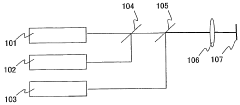
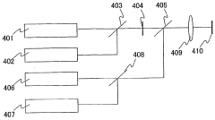
Laser irradiation method, laser irradiation apparatus, and method for manufacturing semiconductor device
PatentWO2005124842A1
Innovation
- The technique involves combining three or more laser beams with different wavelengths using dichroic mirrors and optionally polarizers to create a high-power laser beam with wavelengths in the visible or ultraviolet range, which is then shaped and directed onto a semiconductor substrate for crystallization, allowing for increased productivity and higher output power.
Material Science Implications and Compatibility
Ultrafast laser annealing significantly impacts material properties at the fundamental level, creating unique interactions that differ substantially from conventional thermal processing methods. The extremely short pulse duration (femtoseconds to picoseconds) creates non-equilibrium conditions where energy is delivered to the electron subsystem before transferring to the lattice, allowing for highly localized heating and rapid quenching rates exceeding 10^10 K/s. This distinctive processing regime enables surface modifications without affecting bulk properties, making it particularly valuable for temperature-sensitive materials.
The compatibility of ultrafast laser annealing varies considerably across material classes. Semiconductors like silicon and germanium respond exceptionally well, exhibiting controlled recrystallization and dopant activation with minimal thermal diffusion. This characteristic proves crucial for advanced microelectronics where nanoscale precision is paramount. Metals demonstrate excellent absorption characteristics but require careful parameter optimization to prevent ablation and control surface plasmon effects that can enhance or interfere with the annealing process.
Ceramics and transparent dielectrics present unique challenges due to their wide bandgaps, often necessitating multiphoton absorption mechanisms or the introduction of intermediate absorbing layers. Recent advances in beam shaping and temporal pulse control have expanded the applicability to these traditionally difficult materials. Polymers and organic materials, while historically considered incompatible with laser processing, have shown promising results with ultrafast techniques due to the minimal heat-affected zone.
The material phase transformations induced by ultrafast laser annealing create distinctive microstructures unattainable through conventional processing. These include supersaturated solid solutions, metastable phases, and nanocrystalline structures with enhanced mechanical and electrical properties. The rapid solidification kinetics can suppress segregation and precipitation phenomena, enabling more homogeneous material compositions.
Interface engineering represents another critical aspect of material compatibility. The sharp thermal gradients at material boundaries can either enhance adhesion through diffusion and intermixing or create stress-induced delamination. Recent research has demonstrated successful multilayer annealing protocols that progressively treat complex material stacks while maintaining interface integrity.
Environmental considerations also impact material compatibility, with processing atmosphere (vacuum, inert gas, reactive gas) significantly influencing surface chemistry and oxidation behavior. Humidity levels and ambient contaminants can affect absorption characteristics and resultant surface morphology, necessitating controlled processing environments for reproducible outcomes.
Environmental Impact and Energy Efficiency Considerations
Ultrafast laser annealing technology presents significant environmental and energy efficiency advantages compared to conventional thermal processing methods. The process utilizes extremely short laser pulses in the femtosecond to picosecond range, enabling highly localized heating that substantially reduces the overall energy consumption. Traditional annealing techniques often require heating entire substrates or components to high temperatures for extended periods, whereas ultrafast laser annealing targets only specific surface areas, minimizing unnecessary energy expenditure.
The environmental footprint of ultrafast laser annealing is notably smaller than conventional methods. Studies indicate that energy savings of up to 70-80% can be achieved when compared to furnace-based annealing processes. This reduction stems from the elimination of lengthy heating and cooling cycles, as well as the decreased need for temperature-controlled environments. Additionally, the precise nature of ultrafast laser processing minimizes material waste through optimized surface modification rather than bulk material processing.
Water consumption represents another critical environmental consideration. Conventional annealing often requires significant water resources for cooling systems, while ultrafast laser annealing typically operates with minimal or no water requirements. This aspect becomes increasingly important as water scarcity concerns grow globally, particularly in semiconductor manufacturing regions where water resources are already under pressure.
Chemical usage reduction constitutes a further environmental benefit. Traditional surface treatment methods frequently involve hazardous chemicals for cleaning, etching, or surface preparation. Ultrafast laser annealing can often achieve similar or superior surface modifications without these chemicals, reducing both environmental contamination risks and workplace hazards. Recent research demonstrates that laser-based surface morphology control can replace multiple chemical processing steps in advanced materials manufacturing.
The carbon footprint analysis of ultrafast laser systems reveals promising results when evaluated on a lifecycle basis. While the initial energy investment in laser equipment production is considerable, the operational efficiency over the equipment lifespan typically results in net carbon reductions compared to conventional thermal processing. This advantage becomes more pronounced as renewable energy sources increasingly power manufacturing facilities.
Emerging research focuses on further enhancing the energy efficiency of ultrafast laser annealing through adaptive power management systems. These innovations dynamically adjust laser parameters based on real-time feedback from surface monitoring, ensuring optimal energy delivery for desired morphological changes. Such advancements could potentially reduce energy requirements by an additional 15-25% according to preliminary studies, further strengthening the environmental case for this technology.
Unlock deeper insights with Patsnap Eureka Quick Research — get a full tech report to explore trends and direct your research. Try now!
Generate Your Research Report Instantly with AI Agent
Supercharge your innovation with Patsnap Eureka AI Agent Platform!