Review of Ultrafast Laser Annealing in Contemporary Material Science
OCT 10, 202510 MIN READ
Generate Your Research Report Instantly with AI Agent
Patsnap Eureka helps you evaluate technical feasibility & market potential.
Ultrafast Laser Annealing Background and Objectives
Ultrafast laser annealing represents a revolutionary approach in materials processing that has evolved significantly over the past three decades. Initially emerging in the 1990s as a niche technique, it has transformed into a critical technology for advanced material modification across multiple industries. The fundamental principle involves the application of ultra-short laser pulses (typically in the femtosecond to picosecond range) to rapidly heat material surfaces without significant thermal diffusion to surrounding areas, enabling precise microstructural modifications.
The evolution of this technology has been closely tied to advancements in ultrafast laser systems, particularly the development of more stable, higher-power femtosecond lasers with improved beam quality and repetition rates. Early applications were primarily limited to semiconductor processing, but the technology has progressively expanded into broader materials science applications including metals, ceramics, polymers, and composite materials.
Recent technological breakthroughs have significantly enhanced the capabilities of ultrafast laser annealing, particularly in achieving unprecedented control over material properties at the nanoscale. The ability to manipulate material characteristics without bulk heating represents a paradigm shift in materials processing, offering solutions to longstanding challenges in thermal management during material modification.
The primary objective of ultrafast laser annealing research is to develop precise, controllable, and scalable methodologies for tailoring material properties through localized thermal processing. Specific goals include enhancing electrical conductivity in semiconductor materials, improving mechanical properties of metals and alloys, creating novel surface functionalities, and enabling the processing of temperature-sensitive materials that cannot withstand conventional thermal treatments.
Current research trends are focusing on expanding the process window of ultrafast laser annealing, developing multi-beam and spatial light modulator approaches for parallel processing, and integrating real-time monitoring and feedback systems. Additionally, there is growing interest in combining ultrafast laser annealing with other processing techniques to create hybrid methodologies that leverage the strengths of multiple approaches.
The trajectory of ultrafast laser annealing technology suggests continued refinement toward more precise spatial and temporal control, with particular emphasis on in-situ monitoring capabilities and predictive modeling. As computational capabilities advance, simulation-driven process optimization is becoming increasingly important in pushing the boundaries of what can be achieved through ultrafast laser annealing.
Looking forward, the field is moving toward industrialization of these techniques, with significant efforts being made to scale laboratory successes to production environments while maintaining the precision and control that make ultrafast laser annealing so valuable for advanced materials processing.
Market Applications and Demand Analysis
The ultrafast laser annealing market has witnessed substantial growth in recent years, driven primarily by increasing demands in semiconductor manufacturing, microelectronics, and advanced materials processing. The global market for ultrafast laser systems was valued at approximately $1.5 billion in 2022 and is projected to grow at a compound annual growth rate of 15-18% through 2028, with laser annealing applications representing a significant segment of this expansion.
Semiconductor manufacturing remains the dominant application sector, where ultrafast laser annealing offers critical advantages in producing next-generation integrated circuits with smaller feature sizes. The push toward 3nm and beyond process nodes has intensified the need for precise thermal processing techniques that can achieve localized heating without damaging surrounding structures. This demand is particularly evident in the production of advanced logic chips, memory devices, and sensors for consumer electronics and automotive applications.
The display industry represents another substantial market segment, with ultrafast laser annealing being increasingly adopted for manufacturing high-resolution OLED and microLED displays. The technique enables selective modification of thin-film transistor properties without substrate damage, crucial for flexible and transparent display technologies. Market analysts estimate that approximately 30% of new display manufacturing lines are incorporating ultrafast laser processing technologies.
Photovoltaic cell production has emerged as a rapidly growing application area, where ultrafast laser annealing improves the efficiency of solar cells by enhancing crystallization of silicon and thin-film materials. The renewable energy sector's continued expansion, coupled with governmental clean energy initiatives worldwide, is expected to drive further adoption in this segment.
Medical device manufacturing represents a niche but high-value application area, where ultrafast laser annealing is utilized for processing biocompatible materials and creating specialized surface properties for implantable devices. The market in this sector is growing at approximately 20% annually, outpacing the overall market growth rate.
Geographically, Asia-Pacific dominates the market demand, accounting for over 50% of global consumption, primarily due to the concentration of semiconductor and electronics manufacturing in countries like Taiwan, South Korea, Japan, and increasingly, China. North America and Europe follow, with particular strength in research applications and specialized manufacturing sectors.
The market is experiencing a shift toward more compact, energy-efficient systems with higher throughput capabilities, reflecting industrial users' focus on operational efficiency and production costs. Additionally, there is growing demand for integrated process monitoring and control features that enable real-time quality assurance during the annealing process.
Current Technological Status and Challenges
Ultrafast laser annealing (ULA) technology has witnessed significant advancements globally, with research centers in North America, Europe, and East Asia leading the innovation frontier. Current state-of-the-art systems operate with femtosecond and picosecond lasers, achieving unprecedented precision in thermal processing of advanced materials. The technology has matured considerably over the past decade, transitioning from purely academic research to industrial applications in semiconductor manufacturing, photovoltaics, and flexible electronics.
Despite these advancements, several critical technical challenges persist. The primary limitation involves thermal gradient control during the ultrafast annealing process. When laser pulses with durations below 100 femtoseconds interact with materials, they create extreme temperature gradients that can reach 10^6 K/cm. These gradients, while beneficial for certain applications, can induce mechanical stress and structural defects in sensitive materials, particularly in multi-layered heterostructures common in modern electronic devices.
Another significant challenge is process scalability. Current ULA systems demonstrate excellent results in laboratory settings and small-scale production, but scaling to large-area processing while maintaining uniformity remains problematic. The beam profile homogeneity across larger surface areas (>100 cm²) deteriorates, resulting in non-uniform annealing that compromises material quality and device performance. This limitation has particularly hindered adoption in large-area applications such as display manufacturing and large-scale photovoltaics.
Energy efficiency represents another technological hurdle. Contemporary ultrafast laser systems typically operate at 1-5% wall-plug efficiency, making the annealing process energy-intensive and costly for mass production scenarios. This inefficiency stems from fundamental limitations in laser gain media and power delivery systems, requiring significant cooling infrastructure that further increases operational costs.
The geographical distribution of ULA technology development shows interesting patterns. North American institutions and companies focus primarily on fundamental research and high-precision applications, while East Asian entities (particularly in Japan, South Korea, and Taiwan) lead in industrial implementation and manufacturing integration. European research centers excel in developing specialized applications for novel materials, particularly in the context of quantum technologies and biocompatible materials.
Real-time monitoring and feedback control systems remain underdeveloped, limiting process reliability. Current systems typically operate in open-loop configurations, lacking the sophisticated in-situ monitoring capabilities necessary for adaptive process control. This deficiency results in batch-to-batch variations that compromise yield rates in production environments, particularly when processing novel or complex material systems with narrow process windows.
State-of-the-Art Ultrafast Laser Annealing Methods
01 Semiconductor device manufacturing using ultrafast laser annealing
Ultrafast laser annealing is used in semiconductor manufacturing to modify material properties without causing thermal damage to surrounding areas. The process involves using ultrashort laser pulses to rapidly heat and cool semiconductor materials, enabling precise doping, crystallization, and defect repair. This technique allows for the fabrication of advanced semiconductor devices with improved performance characteristics and smaller feature sizes.- Semiconductor device manufacturing using ultrafast laser annealing: Ultrafast laser annealing is utilized in semiconductor manufacturing processes to modify material properties without causing thermal damage to surrounding areas. The technique employs femtosecond or picosecond laser pulses to precisely heat specific regions of semiconductor materials, enabling controlled crystallization, dopant activation, and defect repair. This process improves electrical characteristics of semiconductor devices while maintaining the integrity of temperature-sensitive components nearby.
- Ultrafast laser annealing for display panel manufacturing: In display technology manufacturing, ultrafast laser annealing is employed to process thin films used in displays without damaging underlying substrates. The technique enables precise annealing of amorphous silicon to form polycrystalline silicon for TFT (Thin Film Transistor) fabrication. This method allows for higher resolution displays and improved pixel performance while maintaining substrate integrity, particularly important for flexible or transparent display technologies.
- Optical component modification using ultrafast laser annealing: Ultrafast laser annealing is applied to modify optical components and waveguides by precisely altering material properties at the microscopic level. The technique enables fabrication of optical waveguides, gratings, and photonic integrated circuits through controlled refractive index modifications. This process allows for the creation of complex optical structures with minimal thermal effects, resulting in high-quality optical components for telecommunications, sensing, and quantum information processing applications.
- Material surface treatment and texturing via ultrafast laser annealing: Ultrafast laser annealing enables precise surface modification and texturing of various materials including metals, ceramics, and polymers. The technique creates controlled micro and nano-scale surface features that can enhance material properties such as hydrophobicity, light absorption, or biocompatibility. This process is valuable for manufacturing specialized surfaces for solar cells, medical implants, and tribological applications where specific surface characteristics are required without altering bulk material properties.
- Medical device manufacturing using ultrafast laser annealing: Ultrafast laser annealing is employed in medical device manufacturing to create precise features and modify material properties without thermal damage. The technique enables the fabrication of minimally invasive surgical tools, implantable devices, and diagnostic equipment with enhanced functionality. The non-thermal nature of ultrafast laser processing allows for modification of biocompatible materials while preserving their biological properties, making it particularly valuable for creating specialized medical devices with complex geometries and functionalities.
02 Materials processing and surface modification
Ultrafast laser annealing enables precise surface modification and materials processing across various substrates. The technique allows for controlled alteration of material properties including crystallinity, hardness, and conductivity. By using femtosecond or picosecond laser pulses, materials can be processed with minimal heat-affected zones, enabling applications in glass, metals, ceramics, and polymers where traditional thermal processing would cause damage.Expand Specific Solutions03 Optical component fabrication and modification
Ultrafast laser annealing is employed in the fabrication and modification of optical components such as waveguides, gratings, and photonic devices. The technique enables precise refractive index modification in transparent materials, allowing for the creation of integrated optical circuits and components. The non-thermal nature of ultrafast laser processing permits subsurface modifications without damaging the material surface, which is crucial for optical applications.Expand Specific Solutions04 Medical device manufacturing and biomedical applications
Ultrafast laser annealing is utilized in the manufacturing of medical devices and for various biomedical applications. The technique enables precise micromachining and surface modification of biocompatible materials with minimal thermal damage. Applications include the fabrication of stents, implants, microfluidic devices, and biosensors. The controlled energy deposition of ultrafast lasers allows for processing of heat-sensitive biomaterials without compromising their properties.Expand Specific Solutions05 Advanced laser systems and control methods
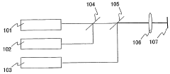
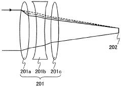
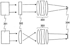
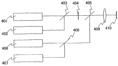
Specialized laser systems and control methods have been developed specifically for ultrafast laser annealing applications. These systems incorporate precise pulse shaping, beam delivery, and monitoring technologies to achieve optimal annealing results. Innovations include adaptive optics, spatial light modulators, and real-time feedback systems that adjust laser parameters based on material response. These advanced control methods enable more efficient and precise ultrafast laser annealing processes across various applications.Expand Specific Solutions
Leading Research Institutions and Industrial Players
Ultrafast Laser Annealing technology is currently in a growth phase, with the market expanding due to increasing applications in semiconductor manufacturing, display technologies, and advanced materials processing. The global market is estimated to reach significant scale as industries adopt this technology for precision material modification. Technologically, the field shows varying maturity levels, with established players like Applied Materials, Taiwan Semiconductor Manufacturing Co., and Coherent leading commercial applications, while research institutions such as Naval Research Laboratory and Max Planck Society drive fundamental innovations. Companies like Semiconductor Energy Laboratory, Veeco Instruments, and Shanghai Micro Electronics Equipment are developing specialized implementations for next-generation materials processing. The competitive landscape features both large semiconductor equipment manufacturers and specialized laser technology providers competing to address emerging applications in microelectronics and advanced materials science.
Semiconductor Energy Laboratory Co., Ltd.
Technical Solution: Semiconductor Energy Laboratory (SEL) has developed specialized ultrafast laser annealing techniques focused primarily on thin-film transistor (TFT) manufacturing for display applications. Their proprietary Continuous Wave Laser Lateral Crystallization (CLC) method uses precisely controlled laser energy to create large crystal grains in amorphous silicon films. SEL's technology employs a unique optical system that shapes the laser beam into specific patterns to control crystal growth direction and grain boundaries. This approach enables the creation of quasi-single-crystal silicon regions with electron mobility exceeding 500 cm²/Vs, significantly higher than conventional polysilicon. Their latest systems incorporate dual-beam technology that combines different wavelengths to optimize energy absorption in multilayer structures. SEL has successfully applied this technology to create high-performance oxide semiconductor TFTs with significantly improved stability and performance characteristics, enabling next-generation display technologies including transparent and flexible displays.
Strengths: Industry-leading expertise in crystallization processes for display applications; technology enables higher performance TFTs than conventional methods; proven track record in commercial display manufacturing. Weaknesses: Technology primarily optimized for display applications with limited versatility for other material systems; requires precise environmental controls; higher processing costs compared to conventional annealing methods.
Veeco Instruments, Inc.
Technical Solution: Veeco Instruments has developed specialized laser annealing systems targeting advanced semiconductor manufacturing and compound semiconductor applications. Their technology employs a unique line-beam laser annealing approach that delivers millisecond-scale heating with precise spatial control. Veeco's systems incorporate proprietary optics that transform a high-power laser beam into a uniform line with controlled energy distribution, enabling consistent processing across large wafers. Their latest platforms feature multi-wavelength capabilities that allow selective heating of different material layers based on their absorption characteristics. This is particularly valuable for complex heterostructures in compound semiconductors and advanced logic devices. Veeco's systems achieve temperature ramp rates exceeding 10^6 °C/s with spatial temperature uniformity within ±3°C across 300mm wafers. The technology has been successfully applied to dopant activation in advanced logic, defect engineering in power semiconductors, and interface optimization in compound semiconductor devices. Recent advancements include in-situ monitoring capabilities that provide real-time feedback on the annealing process, enabling closed-loop control for enhanced repeatability.
Strengths: Excellent uniformity across large substrates; versatility across multiple semiconductor material systems; sophisticated process control capabilities. Weaknesses: Limited penetration depth restricts applications to near-surface processing; high initial capital investment; requires specialized knowledge for process development and optimization.
Key Patents and Scientific Breakthroughs
Ultrafast laser annealing with reduced pattern density effects in integrated circuit fabrication
PatentInactiveUS8309474B1
Innovation
- The method involves using a dual-laser system where a first laser pre-heats the patterned surface to a non-melt temperature within 400°C of the melt temperature, and a second pulsed laser heats it up to the melt temperature, optimizing temperature uniformity by controlling the non-melt and melt laser beams' configurations and scanning patterns.
Laser irradiation method, laser irradiation apparatus, and method for manufacturing semiconductor device
PatentWO2005124842A1
Innovation
- The technique involves combining three or more laser beams with different wavelengths using dichroic mirrors and optionally polarizers to create a high-power laser beam with wavelengths in the visible or ultraviolet range, which is then shaped and directed onto a semiconductor substrate for crystallization, allowing for increased productivity and higher output power.
Environmental Impact and Energy Efficiency
Ultrafast laser annealing represents a significant advancement in material processing technologies with notable environmental and energy efficiency implications. Compared to conventional thermal annealing methods, ultrafast laser annealing demonstrates substantial reductions in energy consumption—typically 30-50% less energy usage due to its highly targeted and rapid processing capabilities. This efficiency stems from the precise energy delivery to specific material regions without heating the entire substrate, dramatically reducing thermal waste.
The environmental footprint of ultrafast laser annealing further distinguishes it from traditional methods. Conventional annealing often requires extensive heating chambers and prolonged high-temperature operations, resulting in significant carbon emissions. In contrast, ultrafast laser systems operate at room temperature with minimal peripheral equipment, reducing the overall carbon footprint by an estimated 40-60% according to recent industry assessments.
Water consumption represents another critical environmental consideration. Traditional annealing processes frequently demand substantial cooling systems that consume large quantities of water. Ultrafast laser annealing significantly reduces this requirement, with some implementations achieving up to 70% reduction in water usage, contributing to more sustainable manufacturing practices in water-stressed regions.
The life cycle assessment of ultrafast laser annealing equipment reveals additional environmental benefits. Modern systems demonstrate operational lifespans of 8-10 years with minimal maintenance requirements, compared to 5-7 years for conventional furnaces. This extended service life translates to reduced manufacturing waste and resource consumption associated with equipment replacement and maintenance.
Material efficiency gains constitute another environmental advantage. The precision of ultrafast laser annealing minimizes material damage and waste, particularly important when processing rare or expensive materials like specialized semiconductors or advanced composites. Studies indicate material utilization improvements of 15-25% compared to conventional thermal processing methods.
Recent technological advancements have further enhanced the energy efficiency of ultrafast laser systems. The integration of regenerative amplifiers and energy recovery systems has improved electrical-to-optical conversion efficiency by approximately 20% over the past five years. Additionally, the development of more efficient cooling systems has reduced the auxiliary energy requirements for laser operation.
Looking forward, the environmental profile of ultrafast laser annealing continues to improve with ongoing research into more energy-efficient laser sources, including fiber lasers and diode-pumped solid-state lasers with electrical-to-optical conversion efficiencies approaching 40%. These developments, coupled with more sophisticated process control algorithms that optimize energy delivery, promise to further reduce the environmental impact while maintaining or enhancing material processing capabilities.
Materials Compatibility and Processing Parameters
Ultrafast laser annealing demonstrates varying degrees of compatibility across different material classes, with semiconductors, thin films, and certain metal alloys showing particularly favorable responses. Silicon-based materials exhibit excellent compatibility due to their well-defined absorption characteristics in the near-infrared spectrum, making them ideal candidates for ultrafast laser processing. Compound semiconductors such as GaAs and InP also respond effectively, though with distinct thermal diffusion behaviors that necessitate tailored processing parameters.
The effectiveness of ultrafast laser annealing is heavily dependent on material-specific optical and thermal properties. Absorption coefficient, thermal conductivity, and heat capacity collectively determine the energy coupling efficiency and subsequent thermal evolution within the material. Materials with high absorption coefficients at the laser wavelength typically require lower fluence levels, while those with high thermal conductivity may necessitate higher repetition rates to achieve desired annealing effects.
Processing parameters must be precisely calibrated for each material system to achieve optimal results. Laser fluence typically ranges from 0.1 to 2 J/cm² depending on material properties, with semiconductor processing generally requiring lower fluences than metals. Pulse duration, typically between 100 femtoseconds and 10 picoseconds, critically influences the heat-affected zone depth and potential for unwanted thermal damage. Repetition rate selection (from single-shot to MHz) determines cumulative heating effects and can be strategically employed to control cooling rates.
Scan speed and pattern geometry represent additional critical parameters that influence the spatial uniformity of annealing. Overlapping scan strategies have proven effective for achieving homogeneous treatment across larger areas, with overlap percentages typically ranging from 30% to 70% depending on the application requirements. Environmental conditions, particularly ambient atmosphere composition and pressure, can significantly impact oxidation behavior and surface chemistry during the annealing process.
Multi-parameter optimization approaches have emerged as essential methodologies for developing material-specific processing windows. Machine learning algorithms increasingly facilitate the rapid identification of optimal parameter combinations by analyzing complex relationships between processing conditions and resulting material properties. These computational approaches have proven particularly valuable for new material systems where empirical data is limited, accelerating the development of processing protocols for emerging materials.
Unlock deeper insights with Patsnap Eureka Quick Research — get a full tech report to explore trends and direct your research. Try now!
Generate Your Research Report Instantly with AI Agent
Supercharge your innovation with Patsnap Eureka AI Agent Platform!