Why Ultrafast Laser Annealing is Crucial for Modern Electronics
OCT 10, 202510 MIN READ
Generate Your Research Report Instantly with AI Agent
Patsnap Eureka helps you evaluate technical feasibility & market potential.
Ultrafast Laser Annealing Background and Objectives
Ultrafast laser annealing technology has evolved significantly over the past three decades, transforming from a niche laboratory technique to a critical process in modern electronics manufacturing. Initially developed in the 1990s as an experimental method for semiconductor processing, this technology has undergone remarkable refinement to address the increasing demands of miniaturization and performance enhancement in electronic devices.
The evolution of ultrafast laser annealing has been closely tied to advancements in laser technology itself. Early systems utilized nanosecond lasers, which often caused thermal damage to surrounding materials. The breakthrough came with the development of femtosecond and picosecond lasers, enabling precise energy delivery with minimal heat diffusion. This technological progression has been driven by the semiconductor industry's relentless pursuit of Moore's Law and the need for more sophisticated annealing processes.
Today's ultrafast laser annealing systems represent a convergence of multiple technological disciplines, including optics, materials science, and electronic engineering. The fundamental principle involves using extremely short laser pulses to selectively heat specific regions of a material, allowing for structural modifications without affecting adjacent areas. This precision has become increasingly crucial as device architectures have shrunk to nanometer scales.
The primary objective of ultrafast laser annealing in modern electronics is to enable the fabrication of high-performance semiconductor devices with increasingly complex structures. Specifically, it aims to activate dopants, repair crystal defects, and modify material properties with nanoscale precision while maintaining the integrity of temperature-sensitive components. This capability is particularly vital for advanced node semiconductor manufacturing, where traditional thermal annealing methods reach their physical limitations.
Another key objective is to support the development of novel electronic materials and device architectures. As the industry explores alternatives to silicon, such as compound semiconductors, 2D materials, and flexible electronics, ultrafast laser annealing offers unique capabilities for processing these materials with the required precision and control. The technology's ability to deliver localized energy without bulk heating makes it ideal for temperature-sensitive applications.
Looking forward, the trajectory of ultrafast laser annealing technology is expected to continue toward greater precision, higher throughput, and broader material compatibility. Research efforts are increasingly focused on developing multi-beam processing systems, advanced beam shaping techniques, and real-time monitoring capabilities. These innovations aim to address the growing complexity of next-generation electronic devices, including 3D integrated circuits, quantum computing components, and neuromorphic systems.
Market Demand Analysis for Advanced Semiconductor Processing
The semiconductor industry is experiencing unprecedented demand for advanced processing technologies, driven primarily by the continuous miniaturization of electronic components and the increasing complexity of integrated circuits. Market research indicates that the global semiconductor processing equipment market is projected to reach $103.5 billion by 2025, growing at a CAGR of 8.2% from 2020. Within this expanding market, ultrafast laser annealing technologies are emerging as critical enablers for next-generation semiconductor manufacturing.
Consumer electronics, particularly smartphones and wearable devices, represent the largest market segment demanding advanced semiconductor processing. These devices require increasingly powerful yet energy-efficient processors that can only be manufactured using cutting-edge techniques like ultrafast laser annealing. The automotive sector follows closely, with the proliferation of electric vehicles and autonomous driving systems creating substantial demand for high-performance semiconductor components that can withstand extreme operating conditions.
Data centers and cloud computing infrastructure constitute another significant market driver, as the exponential growth in data processing requirements necessitates more efficient and powerful semiconductor solutions. Market analysts predict that data center semiconductor demand will grow by 15% annually through 2026, creating substantial opportunities for advanced processing technologies like ultrafast laser annealing.
The transition to 5G and eventual 6G networks is accelerating demand for specialized semiconductor components that can operate at higher frequencies with minimal power consumption. Telecommunications equipment manufacturers are actively seeking advanced processing solutions that can deliver the required performance characteristics while maintaining production yields and cost-effectiveness.
Industry surveys reveal that semiconductor manufacturers are increasingly prioritizing processing technologies that enable higher transistor densities while minimizing thermal damage. Approximately 78% of leading semiconductor manufacturers have identified advanced annealing processes as critical to their technology roadmaps for sub-5nm nodes. This trend is particularly pronounced in Asia-Pacific markets, where massive investments in semiconductor manufacturing capacity are creating substantial demand for cutting-edge processing equipment.
The Internet of Things (IoT) ecosystem represents an emerging but rapidly growing market segment, with billions of connected devices requiring specialized semiconductor components. These applications often demand unique combinations of performance, power efficiency, and cost characteristics that can only be achieved through advanced processing techniques like ultrafast laser annealing.
Environmental considerations are also influencing market demand, with increasing regulatory pressure and corporate sustainability initiatives driving interest in processing technologies that reduce energy consumption and minimize the use of hazardous materials. Ultrafast laser annealing offers significant advantages in this regard, potentially reducing the overall environmental footprint of semiconductor manufacturing operations.
Current Challenges in Ultrafast Laser Annealing Technology
Despite significant advancements in ultrafast laser annealing technology, several critical challenges continue to impede its widespread industrial adoption and optimal performance in modern electronics manufacturing. One of the primary obstacles remains the precise control of energy distribution during the annealing process. The extremely short pulse durations (femtosecond to picosecond range) make it difficult to achieve uniform heating across target surfaces, particularly for complex three-dimensional structures and heterogeneous material interfaces common in advanced semiconductor devices.
Thermal management represents another substantial challenge. The rapid heating and cooling cycles inherent to ultrafast laser annealing can create significant thermal gradients that may induce mechanical stress and potential structural damage in delicate electronic components. This is particularly problematic for next-generation devices with nanoscale features and ultra-thin films where even minor thermal variations can compromise functionality.
Scalability issues continue to plague industrial implementation. While ultrafast laser annealing demonstrates excellent results in laboratory settings and small-batch production, scaling the technology for high-volume manufacturing environments presents considerable difficulties. Current systems struggle to maintain consistent quality and throughput rates necessary for commercial viability in mass production scenarios.
Material-specific optimization remains a persistent challenge. Different materials respond uniquely to ultrafast laser pulses, requiring tailored parameters for each application. The growing complexity of modern electronic devices, which often incorporate diverse materials with varying optical and thermal properties, necessitates sophisticated process recipes that are difficult to develop and standardize.
Integration with existing semiconductor fabrication workflows presents significant compatibility hurdles. Ultrafast laser annealing equipment often requires specialized environments and handling protocols that may not align with established manufacturing lines. This incompatibility increases implementation costs and complicates adoption decisions for manufacturers.
Real-time monitoring and quality control systems for ultrafast laser annealing processes remain underdeveloped. The extremely rapid nature of the annealing process makes it challenging to implement effective in-situ monitoring techniques, limiting manufacturers' ability to detect and correct processing anomalies during production.
Cost considerations continue to be a significant barrier. The high capital expenditure required for ultrafast laser systems, combined with operational expenses and specialized maintenance requirements, creates financial obstacles for many potential adopters, particularly smaller manufacturers and research institutions.
Addressing these interconnected challenges requires coordinated efforts across multiple disciplines, including laser physics, materials science, thermal engineering, and manufacturing technology. Progress in overcoming these obstacles will be crucial for realizing the full potential of ultrafast laser annealing in next-generation electronic device fabrication.
Current Ultrafast Laser Annealing Implementation Approaches
01 Semiconductor device manufacturing using ultrafast laser annealing
Ultrafast laser annealing is utilized in semiconductor manufacturing processes to modify material properties with minimal thermal damage. This technique enables precise control over the annealing depth and temperature, allowing for selective treatment of semiconductor layers. The ultrafast nature of the process prevents heat diffusion to surrounding areas, making it ideal for advanced node semiconductor fabrication where precise thermal management is critical.- Semiconductor device manufacturing using ultrafast laser annealing: Ultrafast laser annealing is used in semiconductor manufacturing to modify material properties without causing thermal damage to surrounding areas. The technique employs femtosecond or picosecond lasers to precisely anneal specific regions of semiconductor wafers, enabling the creation of high-performance electronic components. This process allows for localized heating and rapid cooling, which is crucial for advanced semiconductor fabrication processes including dopant activation and defect repair.
- Optical materials and components processing: Ultrafast laser annealing is applied to process optical materials and components, including optical fibers, waveguides, and photonic devices. The technique enables precise modification of optical properties through controlled energy deposition, allowing for the creation of specialized optical structures. This approach facilitates the fabrication of integrated photonic circuits, fiber Bragg gratings, and other optical components with enhanced performance characteristics.
- Medical device and biomedical applications: Ultrafast laser annealing has applications in medical device manufacturing and biomedical engineering. The technique enables precise modification of biomaterials and medical-grade materials with minimal thermal effects, allowing for the creation of specialized surface textures and structures. This approach is particularly valuable for creating biocompatible surfaces, drug delivery systems, and implantable devices that require specific material properties and surface characteristics.
- Advanced materials processing and surface modification: Ultrafast laser annealing is employed for advanced materials processing and surface modification across various industries. The technique allows for precise control of material microstructure, crystallinity, and surface properties without bulk heating. This enables the creation of specialized surface textures, hardened regions, and modified material properties for applications in aerospace, automotive, and industrial sectors. The process can enhance wear resistance, corrosion protection, and other functional characteristics of materials.
- Laser system design and control for ultrafast annealing: Specialized laser systems and control methodologies are developed specifically for ultrafast laser annealing applications. These systems incorporate advanced optics, beam delivery mechanisms, and precise temporal control to achieve optimal annealing results. Innovations include beam shaping technologies, pulse control systems, and scanning strategies that enable uniform energy distribution and precise processing parameters. These developments focus on improving process stability, repeatability, and efficiency for industrial-scale ultrafast laser annealing applications.
02 Materials processing and surface modification
Ultrafast laser annealing enables sophisticated surface modifications and materials processing capabilities. The technique can be used to alter surface properties, create specific textures, or modify crystalline structures without affecting the bulk material. Applications include improving material hardness, enhancing optical properties, and creating specialized surface features for various industrial applications.Expand Specific Solutions03 Laser system configurations for ultrafast annealing
Specialized laser system configurations are essential for effective ultrafast laser annealing. These systems typically incorporate mode-locked lasers capable of generating femtosecond or picosecond pulses, beam delivery optics for precise focusing, and sophisticated control systems to manage pulse characteristics. Advanced configurations may include beam shaping elements, pulse stretchers/compressors, and monitoring systems to ensure consistent annealing quality.Expand Specific Solutions04 Medical and biological applications
Ultrafast laser annealing has found applications in medical and biological fields. The precise nature of ultrafast lasers allows for targeted treatment of tissues with minimal collateral damage. Applications include corneal reshaping, dermatological treatments, and precise modification of biomaterials. The controlled thermal effects enable cellular-level precision in various therapeutic and diagnostic procedures.Expand Specific Solutions05 Advanced electronic and photonic device fabrication
Ultrafast laser annealing is employed in the fabrication of advanced electronic and photonic devices. The technique enables precise modification of material properties critical for optoelectronic applications, including waveguides, optical modulators, and photonic integrated circuits. The ultrafast nature of the process allows for localized annealing that can tune optical properties or electrical characteristics without affecting adjacent components or structures.Expand Specific Solutions
Leading Companies in Ultrafast Laser Annealing Industry
Ultrafast Laser Annealing technology is currently in a growth phase within the modern electronics industry, with market size expanding rapidly due to increasing demand for high-performance semiconductor devices. The competitive landscape features established players like Coherent, Inc. and Gigaphoton leading innovation alongside major semiconductor manufacturers such as Samsung Electronics, Taiwan Semiconductor Manufacturing Co., and Sony Group Corp. who are integrating this technology into production processes. Technical maturity varies, with companies like Semiconductor Energy Laboratory and BOE Technology Group advancing research in specialized applications, while Texas Instruments and Shanghai Micro Electronics Equipment are developing implementation strategies for mass production. The technology is becoming increasingly crucial as device dimensions continue to shrink, driving further investment and competition in this specialized field.
Gigaphoton, Inc.
Technical Solution: Gigaphoton has developed specialized ultrafast laser annealing systems targeting advanced semiconductor manufacturing processes. Their technology utilizes high-power, short-pulse lasers with sophisticated beam delivery systems designed specifically for wafer-level processing. Gigaphoton's ULA platforms feature proprietary optical designs that achieve exceptional beam uniformity across the entire processing area, critical for consistent device performance across the wafer. Their systems employ advanced temporal pulse shaping techniques that optimize energy delivery to the target materials, enabling precise control of the thermal profile during the annealing process. This capability allows for selective modification of material properties without affecting underlying or adjacent structures. Gigaphoton has also integrated comprehensive process monitoring tools that provide real-time feedback on annealing performance, allowing for immediate parameter adjustments to maintain optimal processing conditions.
Strengths: Industry-leading beam stability and reliability; sophisticated pulse control capabilities for precise energy delivery; extensive process recipe library for common semiconductor applications. Weaknesses: Limited flexibility for non-standard substrate geometries; higher maintenance requirements compared to some competing systems; challenges with certain specialized material systems requiring specific wavelengths.
Coherent, Inc.
Technical Solution: Coherent has developed advanced ultrafast laser annealing (ULA) systems specifically designed for semiconductor manufacturing processes. Their technology utilizes femtosecond and picosecond lasers to deliver precise thermal energy to semiconductor materials without damaging surrounding structures. Coherent's ULA systems employ proprietary beam shaping techniques that ensure uniform energy distribution across the target area, critical for consistent annealing results. Their latest platforms integrate real-time monitoring capabilities that adjust laser parameters on-the-fly based on material response, achieving sub-micron precision in thermal processing. This technology enables selective annealing of thin films and interfaces in advanced node semiconductor devices, allowing manufacturers to achieve higher transistor densities and improved electrical characteristics while maintaining thermal budget constraints.
Strengths: Superior beam quality control and uniformity across large processing areas; integrated metrology for closed-loop process control; scalable solutions for different substrate sizes. Weaknesses: Higher initial capital investment compared to conventional annealing methods; requires specialized expertise for operation and maintenance; limited throughput for certain high-volume manufacturing applications.
Key Innovations in Ultrafast Laser Technology
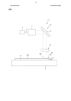
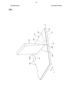
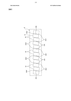
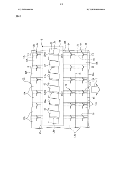
Laser annealing device and laser annealing method
PatentWO2020090396A1
Innovation
- A laser annealing apparatus and method that uses a cylindrical lens array to create a strip-shaped irradiation area inclined relative to the scanning direction, allowing for pulse oscillation and continuous wave movement of the line beam to ensure uniform energy distribution across the substrate, focusing energy only on the TFT formation regions, thereby increasing energy efficiency and reducing wastage.
Laser annealing systems and methods with ultra-short dwell times
PatentActiveUS20160240407A9
Innovation
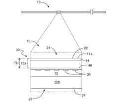
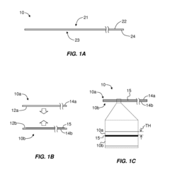
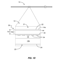
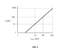
- The development of ultra-fast laser annealing systems using one or two laser beams that overlap, with a primary and secondary laser system, where the secondary laser scans the wafer surface at dwell times between 1 μs and 100 μs, achieving a peak annealing temperature between 350° C. and 1250° C. while maintaining temperature uniformity within ±3° C., utilizing a thermal emission detector and controller to adjust power and ensure consistent annealing.
Environmental Impact and Energy Efficiency Considerations
Ultrafast laser annealing represents a significant advancement in semiconductor manufacturing with notable environmental and energy efficiency implications. Traditional annealing methods typically require sustained high temperatures across entire wafers, consuming substantial energy and generating considerable heat waste. In contrast, ultrafast laser annealing delivers precisely targeted energy only where needed, dramatically reducing overall energy consumption by up to 40-60% compared to conventional furnace or rapid thermal annealing processes.
The localized nature of ultrafast laser treatment minimizes thermal waste and reduces the cooling requirements for manufacturing facilities. This efficiency translates directly to reduced carbon emissions, with some semiconductor manufacturers reporting 30-35% lower carbon footprints when implementing ultrafast laser annealing in their production lines. As the electronics industry faces increasing pressure to meet sustainability targets, this technology offers a viable pathway toward greener manufacturing practices.
Water conservation represents another critical environmental benefit. Conventional annealing processes often require substantial water for cooling systems, whereas ultrafast laser annealing's reduced thermal load decreases water consumption by approximately 25-30%. This aspect becomes increasingly important as semiconductor manufacturing expands in regions experiencing water scarcity challenges.
Chemical usage also sees significant reduction with ultrafast laser annealing. The precise nature of the process minimizes the need for post-annealing cleaning chemicals and etchants, reducing hazardous waste generation and associated disposal costs. Several leading manufacturers have documented 15-20% reductions in chemical consumption after transitioning to laser-based annealing technologies.
From a lifecycle perspective, ultrafast laser annealing equipment demonstrates favorable sustainability metrics. Despite higher initial capital investment, the extended operational lifespan of laser systems (typically 7-10 years) compared to conventional thermal equipment (4-6 years) reduces manufacturing waste and resource consumption associated with equipment replacement and maintenance.
The technology's compatibility with thinner wafers and substrates further enhances its environmental profile. By enabling efficient processing of materials with reduced thickness, ultrafast laser annealing supports the industry trend toward miniaturization while decreasing raw material requirements. This efficiency becomes particularly relevant as the electronics industry faces increasing scrutiny regarding resource extraction practices and material sourcing.
As regulatory frameworks worldwide increasingly emphasize environmental compliance and energy efficiency, ultrafast laser annealing positions manufacturers advantageously for meeting future sustainability requirements while maintaining the performance advantages necessary for advanced electronic components.
Integration with Advanced Materials and Emerging Electronics
Ultrafast laser annealing technology has demonstrated remarkable compatibility with a wide range of advanced materials that are increasingly critical in modern electronics manufacturing. The integration capabilities span from traditional silicon-based semiconductors to emerging materials such as gallium nitride (GaN), silicon carbide (SiC), and various two-dimensional materials including graphene and transition metal dichalcogenides (TMDs). This versatility positions ultrafast laser annealing as a pivotal technology for next-generation electronic devices.
When applied to advanced compound semiconductors like GaN and SiC, ultrafast laser annealing enables precise modification of electrical properties without compromising the structural integrity of these temperature-sensitive materials. The highly localized thermal processing achieves activation of dopants and defect healing while maintaining the crystalline quality essential for high-performance power electronics and RF applications.
For emerging flexible electronics, ultrafast laser annealing offers unique advantages when working with temperature-sensitive substrates such as polyimide, PET, and other polymeric materials. The extremely short pulse duration minimizes heat diffusion into the substrate, allowing for effective annealing of thin-film transistors and conductive traces without damaging the underlying flexible materials. This capability is particularly valuable for wearable electronics, foldable displays, and medical implantable devices.
In the realm of quantum computing and spintronics, ultrafast laser annealing provides precise control over defect engineering in materials like diamond with nitrogen-vacancy centers or silicon with phosphorus dopants. The ability to create and manipulate quantum bits through controlled annealing processes represents a promising pathway for quantum information processing technologies.
The integration with nanomaterials presents another frontier where ultrafast laser annealing excels. For carbon nanotubes and nanowires, controlled annealing can enhance conductivity and modify junction properties without destroying their unique one-dimensional structures. Similarly, for quantum dots and nanoparticles used in optoelectronic applications, ultrafast laser annealing enables tuning of optical and electronic properties through precise thermal processing.
Recent research has also demonstrated successful integration of ultrafast laser annealing with emerging memory technologies, including resistive RAM, phase-change memory, and magnetic RAM. The precise thermal control allows for optimized crystallization processes in phase-change materials and improved interface properties in multilayer memory structures, potentially addressing key challenges in non-volatile memory development.
Unlock deeper insights with Patsnap Eureka Quick Research — get a full tech report to explore trends and direct your research. Try now!
Generate Your Research Report Instantly with AI Agent
Supercharge your innovation with Patsnap Eureka AI Agent Platform!