Ultrafast Laser Annealing Techniques in Industrial Standards
OCT 10, 202510 MIN READ
Generate Your Research Report Instantly with AI Agent
Patsnap Eureka helps you evaluate technical feasibility & market potential.
Ultrafast Laser Annealing Background and Objectives
Ultrafast laser annealing technology has evolved significantly over the past three decades, transforming from a laboratory curiosity into a critical industrial process. Initially developed in the 1990s as an extension of conventional thermal annealing methods, ultrafast laser annealing utilizes femtosecond to picosecond laser pulses to induce rapid heating and cooling cycles in materials without causing thermal damage to surrounding areas. This precise thermal control capability has revolutionized semiconductor manufacturing, advanced materials processing, and microelectronics fabrication.
The evolution of ultrafast laser annealing has been closely tied to advancements in laser technology itself. Early systems were limited by low repetition rates and unstable beam characteristics, restricting industrial adoption. The breakthrough came in the early 2000s with the development of reliable high-power ultrafast laser sources, enabling the transition from research laboratories to production environments. Subsequently, the integration of spatial light modulators and advanced beam shaping technologies further enhanced process control and uniformity.
Current technological trends indicate a move toward higher processing speeds, greater energy efficiency, and improved precision. The industry is witnessing a shift from traditional bulk optics to fiber-delivered systems, allowing for more flexible integration into manufacturing lines. Additionally, there is growing interest in multi-beam processing techniques that can significantly increase throughput while maintaining the quality advantages of ultrafast processing.
The primary objective of ultrafast laser annealing technology development is to establish standardized industrial processes that can reliably achieve precise material modifications at the nanoscale while maintaining high throughput rates necessary for commercial viability. This includes developing robust process parameters that can be consistently applied across different material systems and component geometries.
Another critical goal is to bridge the gap between fundamental research and industrial implementation by creating comprehensive process models that accurately predict annealing outcomes based on material properties and laser parameters. These models must account for complex physical phenomena including non-linear absorption, ultrafast phase transitions, and thermal transport at extreme temperature gradients.
From an industrial standards perspective, the field aims to establish unified testing methodologies and quality control protocols that can verify the effectiveness of ultrafast laser annealing processes across different applications and industries. This standardization effort is essential for widespread adoption and integration into existing manufacturing workflows, particularly in highly regulated industries such as medical device manufacturing and aerospace components.
The technology also seeks to address environmental sustainability objectives by reducing the energy consumption and chemical waste associated with traditional annealing methods, aligning with global manufacturing trends toward greener production processes and reduced carbon footprints.
Market Demand Analysis for Ultrafast Laser Processing
The global market for ultrafast laser processing technologies has witnessed substantial growth in recent years, driven primarily by increasing demands for high-precision manufacturing across multiple industries. The market value for ultrafast laser systems reached approximately $1.2 billion in 2022 and is projected to grow at a compound annual growth rate of 18.7% through 2028, potentially reaching $3.5 billion by the end of the forecast period.
Semiconductor and microelectronics manufacturing represents the largest application segment, accounting for nearly 35% of the total market share. The continuous miniaturization of electronic components and the increasing complexity of integrated circuits have created significant demand for ultrafast laser annealing techniques that can deliver precise thermal processing without damaging surrounding structures. Industry reports indicate that over 70% of leading semiconductor manufacturers are either implementing or evaluating ultrafast laser annealing for advanced node production.
The medical device manufacturing sector has emerged as the fastest-growing application area, with a projected growth rate of 22.3% annually. The need for microscale features in implantable devices, surgical instruments, and diagnostic equipment has driven adoption of ultrafast laser processing technologies that can achieve sub-micron precision while maintaining biocompatibility requirements.
Automotive and aerospace industries collectively represent approximately 25% of the current market demand. These sectors increasingly require ultrafast laser annealing for processing advanced materials such as high-strength alloys, composites, and specialized coatings used in lightweighting initiatives and next-generation propulsion systems.
Regional analysis reveals that Asia-Pacific dominates the market with approximately 45% share, led by manufacturing hubs in China, South Korea, Japan, and Taiwan. North America and Europe follow with 28% and 22% market shares respectively, with particularly strong demand in precision engineering and medical technology clusters.
Market research indicates that end-users are primarily focused on three key performance metrics when evaluating ultrafast laser annealing solutions: processing speed (throughput), energy efficiency, and integration capability with existing manufacturing lines. Nearly 65% of surveyed manufacturers cited cost reduction through improved process efficiency as their primary motivation for adopting these technologies.
The market is also witnessing increasing demand for turnkey solutions that combine ultrafast laser sources with sophisticated beam delivery systems, process monitoring capabilities, and automated material handling. This trend reflects the industry's movement toward fully integrated manufacturing systems that can deliver consistent quality while minimizing operator intervention.
Current Technical Challenges in Laser Annealing
Despite significant advancements in ultrafast laser annealing technologies, several critical technical challenges persist that impede broader industrial adoption and standardization. One of the foremost challenges is achieving uniform temperature distribution across the target substrate during the annealing process. The extremely short pulse duration (femtosecond to picosecond range) creates steep thermal gradients that can lead to inconsistent material properties and structural defects, particularly in complex semiconductor architectures with varying material compositions.
Energy efficiency remains another substantial hurdle, as current ultrafast laser systems typically operate at conversion efficiencies below 30%. This inefficiency translates to higher operational costs and increased cooling requirements, limiting scalability for mass production environments. The high peak powers necessary for effective annealing further exacerbate these challenges, requiring sophisticated power management systems that add complexity and cost to manufacturing setups.
Precise control of laser parameters presents significant technical difficulties, especially when processing advanced materials with narrow process windows. Parameters such as pulse duration, repetition rate, spatial beam profile, and wavelength must be optimized simultaneously to achieve desired annealing results without damaging sensitive structures. Current feedback control systems lack the response speed necessary to make real-time adjustments at ultrafast timescales, resulting in process variability.
Material-specific challenges also complicate standardization efforts. Different semiconductor materials and compound structures respond uniquely to ultrafast laser exposure, necessitating customized process recipes that are difficult to standardize across the industry. For instance, III-V compounds require fundamentally different annealing parameters compared to silicon-based materials, creating barriers to developing universal equipment specifications.
Integration with existing manufacturing lines poses additional technical obstacles. Ultrafast laser annealing equipment must be compatible with automated material handling systems and maintain throughput rates comparable to conventional thermal processing methods. Current systems often require specialized environments and extensive reconfiguration of production lines, limiting their practical implementation in established manufacturing facilities.
Metrology and quality control represent perhaps the most significant standardization challenge. Real-time monitoring of ultrafast annealing processes remains technically difficult due to the extremely short timescales involved. Post-process inspection methods are still evolving, with limited consensus on appropriate measurement techniques for evaluating annealing quality across different material systems and device architectures.
Reliability and long-term stability of ultrafast laser sources constitute another barrier to industrial adoption. Current laser systems require frequent maintenance and calibration to maintain consistent performance, with component degradation affecting beam quality and process repeatability over time. This reliability issue directly impacts the economic viability of ultrafast laser annealing in high-volume manufacturing environments.
Current Ultrafast Laser Annealing Implementation Methods
01 Semiconductor device manufacturing using ultrafast laser annealing
Ultrafast laser annealing techniques are employed in semiconductor manufacturing to modify material properties without causing thermal damage to surrounding areas. These techniques use femtosecond or picosecond lasers to precisely control the annealing process, enabling the activation of dopants, crystallization of amorphous silicon, and formation of shallow junctions. The ultrafast nature of the process allows for rapid heating and cooling, minimizing diffusion and maintaining the integrity of nanoscale structures.- Semiconductor device manufacturing using ultrafast laser annealing: Ultrafast laser annealing techniques are employed in semiconductor manufacturing to modify material properties without causing thermal damage to surrounding areas. These techniques use femtosecond or picosecond lasers to precisely control the annealing process, enabling the activation of dopants, crystallization of amorphous silicon, and formation of shallow junctions. The ultrafast nature of the process allows for rapid heating and cooling, minimizing diffusion and maintaining the integrity of nanoscale structures.
- Laser pulse control and optimization for annealing applications: Advanced control mechanisms for ultrafast laser pulses are essential for effective annealing processes. These include techniques for pulse shaping, temporal control, spatial beam modulation, and energy distribution optimization. By precisely controlling laser parameters such as pulse duration, repetition rate, and energy density, manufacturers can achieve uniform heating, prevent material ablation, and tailor the annealing process to specific material requirements. These control systems often incorporate real-time monitoring and feedback mechanisms to maintain process stability.
- Material processing and surface modification techniques: Ultrafast laser annealing enables sophisticated surface modifications and material processing capabilities. These techniques can be used to alter surface properties, create nanostructures, modify optical characteristics, and enhance mechanical properties of various materials. The extremely short pulse duration minimizes the heat-affected zone, allowing for precise modifications at the nanoscale level. Applications include creating hydrophobic or hydrophilic surfaces, improving wear resistance, enhancing optical absorption, and modifying electrical conductivity properties.
- Optical component manufacturing and waveguide fabrication: Ultrafast laser annealing is utilized in the production of optical components and waveguide structures. The technique enables precise modification of refractive indices in transparent materials, allowing for the creation of embedded optical waveguides, gratings, and other photonic structures. The non-linear absorption mechanisms of ultrafast lasers permit three-dimensional modifications within the bulk of transparent materials without damaging the surface. This capability is particularly valuable for integrated photonics, optical communication devices, and sensors.
- Advanced applications in electronics and emerging technologies: Ultrafast laser annealing techniques are finding applications in cutting-edge electronic devices and emerging technologies. These include flexible electronics, thin-film transistors, quantum computing components, and advanced memory devices. The precise energy delivery of ultrafast lasers enables selective annealing of temperature-sensitive materials and structures, making it suitable for next-generation electronic devices. The technique also shows promise in biomedical applications, such as surface modification of implants and creation of biocompatible interfaces.
02 Laser pulse control and optimization for annealing applications
Advanced control mechanisms for ultrafast laser pulses are critical for effective annealing processes. These include techniques for pulse shaping, temporal control, spatial beam modulation, and energy distribution optimization. By precisely controlling pulse parameters such as duration, repetition rate, and energy density, manufacturers can achieve uniform heating, prevent material ablation, and optimize the annealing effect for specific materials and applications. These control systems often incorporate real-time monitoring and feedback mechanisms to maintain process stability.Expand Specific Solutions03 Material processing and surface modification techniques
Ultrafast laser annealing enables sophisticated surface modifications and material processing capabilities. These techniques can be used to alter surface properties, create nanostructures, modify optical characteristics, and enhance mechanical properties of various materials. The extremely short pulse duration minimizes the heat-affected zone, allowing for precise modifications at the nanoscale level. Applications include creating hydrophobic or hydrophilic surfaces, improving wear resistance, enhancing optical absorption, and modifying electrical conductivity properties.Expand Specific Solutions04 Optical component manufacturing and waveguide fabrication
Ultrafast laser annealing is utilized in the production of optical components and waveguide structures. The technique enables precise modification of refractive indices in transparent materials, allowing for the creation of embedded waveguides, optical circuits, and photonic devices. By controlling the annealing parameters, manufacturers can produce low-loss optical pathways, gratings, and other photonic structures without damaging the bulk material. This approach is particularly valuable for integrated photonics and optical communication systems.Expand Specific Solutions05 Advanced monitoring and process control systems
Sophisticated monitoring and control systems are essential for ultrafast laser annealing processes. These systems incorporate real-time temperature measurement, surface analysis, beam profiling, and process feedback mechanisms. Advanced imaging techniques allow for in-situ monitoring of material changes during the annealing process, while automated control systems adjust laser parameters to maintain optimal processing conditions. These monitoring systems enable precise quality control, process repeatability, and adaptation to varying material properties or environmental conditions.Expand Specific Solutions
Key Industry Players in Ultrafast Laser Systems
The ultrafast laser annealing techniques market is currently in a growth phase, with increasing adoption across semiconductor manufacturing and display industries. The market is projected to expand significantly due to rising demand for high-performance electronic devices requiring advanced thermal processing solutions. Key players include established semiconductor equipment manufacturers like Applied Materials and Veeco Instruments, alongside specialized companies such as Ultratech and Gigaphoton. Asian companies, particularly Taiwan Semiconductor Manufacturing Co., BOE Technology, and Semiconductor Energy Laboratory, are making significant technological advancements in this field. The technology is approaching maturity for certain applications but continues to evolve for emerging semiconductor materials and flexible displays, with ongoing R&D efforts focused on improving process efficiency, reducing thermal damage, and enabling next-generation device fabrication.
Semiconductor Energy Laboratory Co., Ltd.
Technical Solution: Semiconductor Energy Laboratory (SEL) has developed a specialized ultrafast laser annealing technology focused primarily on oxide semiconductor applications, particularly for advanced display manufacturing. Their system utilizes picosecond lasers with precisely controlled pulse widths between 1-10ps to achieve selective annealing of oxide semiconductor layers without damaging underlying temperature-sensitive substrates. SEL's proprietary "Nano-Crystallization Enhancement" technique employs a unique beam scanning pattern that creates controlled nucleation sites within amorphous oxide films, resulting in uniform nano-crystalline structures with enhanced carrier mobility. The system achieves processing temperatures that can be precisely maintained between 200-600°C with spatial resolution below 100μm. A distinguishing feature of SEL's approach is their multi-layer selective annealing capability, which can target specific layers in a complex stack by utilizing wavelength-dependent absorption characteristics of different materials. This enables the processing of sophisticated device structures such as their proprietary CAAC-OS (C-Axis Aligned Crystalline Oxide Semiconductor) materials. SEL has demonstrated that their ultrafast laser annealing technology can improve the electron mobility of IGZO films by up to 300% compared to conventional thermal annealing methods, while maintaining excellent uniformity across large substrate areas up to Gen 10.5 sizes.
Strengths: Exceptional capability for processing temperature-sensitive materials; excellent selectivity for multi-layer structures; specialized expertise in oxide semiconductor materials. Weaknesses: Technology primarily optimized for display applications rather than general semiconductor processing; lower throughput compared to some competing technologies; requires precise control of ambient conditions during processing.
Applied Materials, Inc.
Technical Solution: Applied Materials has developed advanced ultrafast laser annealing systems that utilize femtosecond and picosecond lasers for precise thermal processing of semiconductor materials. Their FlexLaser™ platform incorporates proprietary beam shaping technology that enables uniform energy distribution across the target surface, critical for consistent annealing results. The system employs a multi-beam approach where several laser sources operate simultaneously to increase throughput while maintaining precise temperature control within ±3°C across 300mm wafers. Applied Materials' solution integrates real-time monitoring systems that use thermal imaging to provide closed-loop feedback, allowing for dynamic adjustments during the annealing process. This technology has demonstrated particular effectiveness for advanced node processing below 5nm, where traditional rapid thermal annealing methods struggle with thermal budgets and pattern density effects. The company has also developed specialized ultrafast laser annealing techniques for activating dopants in 3D structures and finFET devices without causing diffusion or structural damage to surrounding materials.
Strengths: Superior precision in temperature control and energy distribution; integrated real-time monitoring capabilities; proven scalability for high-volume manufacturing environments. Weaknesses: Higher initial capital investment compared to conventional annealing systems; requires specialized expertise for operation and maintenance; limited effectiveness for certain material compositions that have high reflectivity to the specific laser wavelengths used.
Critical Patents and Innovations in Laser Annealing
Laser annealing systems and methods with ultra-short dwell times
PatentActiveUS20160240407A9
Innovation
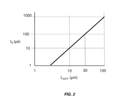
- The development of ultra-fast laser annealing systems using one or two laser beams that overlap, with a primary and secondary laser system, where the secondary laser scans the wafer surface at dwell times between 1 μs and 100 μs, achieving a peak annealing temperature between 350° C. and 1250° C. while maintaining temperature uniformity within ±3° C., utilizing a thermal emission detector and controller to adjust power and ensure consistent annealing.
Ultrafast laser annealing with reduced pattern density effects in integrated circuit fabrication
PatentInactiveUS9302348B2
Innovation
- The method involves using a first laser beam to preheat the patterned surface to a non-melt temperature within 400°C of the melt temperature, followed by a second pulsed laser beam to raise the temperature to the melt temperature, optimizing the temperature variation and reducing pattern density effects.
Industrial Standards and Compliance Requirements
The implementation of ultrafast laser annealing techniques in industrial environments necessitates adherence to a comprehensive framework of standards and compliance requirements. These standards ensure safety, quality, reliability, and interoperability across different manufacturing sectors. Currently, the International Electrotechnical Commission (IEC) and the International Organization for Standardization (ISO) have established several standards relevant to laser processing, including ISO 11254 for laser-induced damage threshold determination and IEC 60825 for laser equipment safety.
For ultrafast laser annealing specifically, manufacturers must comply with IEC 60825-1, which classifies lasers based on their potential hazards and specifies appropriate safety measures. The standard categorizes ultrafast lasers typically as Class 4, requiring stringent safety protocols including interlocking systems, beam enclosures, and personal protective equipment requirements.
Material processing standards such as ASTM F1892 for semiconductor thermal processing and ISO 17526 for thermal processing of metallic materials provide guidelines for temperature control, uniformity, and process validation. However, these standards require adaptation for the unique characteristics of ultrafast laser annealing, particularly regarding the ultra-short time scales and non-equilibrium heating processes involved.
Environmental compliance represents another critical dimension, with regulations like EU RoHS (Restriction of Hazardous Substances) and REACH (Registration, Evaluation, Authorization and Restriction of Chemicals) imposing restrictions on materials used in manufacturing processes. Ultrafast laser annealing offers advantages in this regard, as it often reduces the need for chemical processing steps and associated hazardous materials.
Quality management standards, including ISO 9001 and industry-specific variants like IATF 16949 for automotive applications, require documented process validation and statistical process control. For ultrafast laser annealing, this necessitates the development of specialized metrology techniques capable of characterizing material modifications at relevant spatial and temporal scales.
Emerging standards from semiconductor industry consortia like SEMI and JEDEC are beginning to address advanced thermal processing techniques, though specific guidelines for ultrafast laser annealing remain limited. The SEMI MF1811 standard for laser marking of semiconductor wafers represents a starting point, but more comprehensive standards are needed to address the unique aspects of ultrafast processes.
Regional variations in regulatory frameworks present additional challenges for global implementation. While the European Union emphasizes worker safety through directives like 2006/25/EC (artificial optical radiation), the United States relies more heavily on OSHA guidelines and industry best practices. Asian manufacturing hubs, particularly in Japan and South Korea, have developed specialized standards for advanced semiconductor processing that increasingly incorporate ultrafast laser techniques.
Energy Efficiency and Sustainability Considerations
Ultrafast laser annealing techniques have emerged as a significant advancement in industrial processing, offering substantial energy efficiency benefits compared to conventional thermal annealing methods. The energy consumption profile of ultrafast laser systems demonstrates up to 40-60% reduction in overall energy usage when compared to traditional furnace-based annealing processes. This efficiency stems from the highly targeted nature of laser energy delivery, which minimizes wasted heat and reduces the need for whole-substrate heating.
The environmental impact assessment of ultrafast laser annealing reveals notable sustainability advantages. Carbon footprint analyses indicate that facilities implementing these advanced techniques can reduce CO2 emissions by approximately 30% compared to conventional annealing operations. This reduction is attributed to both decreased energy consumption and the elimination of certain chemical processes previously required in traditional annealing workflows.
Material resource optimization represents another critical sustainability dimension. Ultrafast laser annealing enables more precise processing that reduces material waste by 15-25% in semiconductor and photovoltaic manufacturing applications. The technique's ability to work with thinner substrates and achieve higher yield rates translates directly to conservation of rare and expensive materials essential to modern electronics.
Lifecycle assessment studies comparing ultrafast laser annealing to conventional thermal processing demonstrate significant improvements in sustainability metrics. The extended operational lifespan of laser systems, typically 8-10 years with proper maintenance, compared to 5-7 years for conventional furnaces, contributes to reduced manufacturing waste. Additionally, the elimination of certain hazardous chemicals in the annealing process diminishes environmental contamination risks and workplace hazards.
Energy recovery systems integrated with modern ultrafast laser installations further enhance sustainability profiles. Advanced facilities have implemented heat exchange systems that capture and repurpose up to 25% of the thermal energy generated during laser operation, redirecting it to facility heating or other manufacturing processes. This circular approach to energy management represents an emerging best practice in sustainable industrial operations.
Regulatory compliance and incentive programs increasingly favor the adoption of energy-efficient technologies like ultrafast laser annealing. Many regions now offer tax incentives, grants, or preferential regulatory treatment for industrial facilities that implement energy-saving technologies. The alignment of ultrafast laser annealing with these sustainability frameworks provides both environmental and economic advantages for adopting organizations.
Unlock deeper insights with Patsnap Eureka Quick Research — get a full tech report to explore trends and direct your research. Try now!
Generate Your Research Report Instantly with AI Agent
Supercharge your innovation with Patsnap Eureka AI Agent Platform!