Research on the Effects of Ultrafast Laser Annealing on Superconductors
OCT 10, 20259 MIN READ
Generate Your Research Report Instantly with AI Agent
Patsnap Eureka helps you evaluate technical feasibility & market potential.
Ultrafast Laser Annealing in Superconductivity: Background and Objectives
Ultrafast laser annealing represents a cutting-edge technique in materials science that has evolved significantly over the past two decades. This process utilizes femtosecond or picosecond laser pulses to rapidly heat and cool materials, allowing for precise modification of their microstructure without excessive thermal diffusion to surrounding areas. When applied to superconductors, this technique offers unprecedented control over material properties at the nanoscale.
The historical development of ultrafast laser technology began in the 1990s with the advent of reliable femtosecond laser systems. However, its application to superconducting materials gained momentum only in the early 2000s when researchers recognized its potential for controlled modification of critical parameters such as transition temperature (Tc) and critical current density (Jc).
Superconductivity itself has undergone several revolutionary phases since its discovery by Kamerlingh Onnes in 1911. The field experienced major breakthroughs with the discovery of high-temperature superconductors in the 1980s and iron-based superconductors in the 2000s. Despite these advances, practical applications remain limited by processing challenges and material performance constraints.
The intersection of ultrafast laser technology and superconductivity presents a promising frontier. Traditional annealing methods for superconductors typically involve bulk heating processes that lack spatial precision and can introduce unwanted thermal stress. Ultrafast laser annealing offers a non-equilibrium processing route that can potentially overcome these limitations through highly localized energy deposition.
Current technological trends indicate growing interest in quantum computing, medical imaging, and energy transmission systems—all areas where advanced superconducting materials could provide transformative solutions. The ability to fine-tune superconducting properties through precise laser processing aligns perfectly with these emerging application needs.
The primary objectives of research in this field include: understanding the fundamental mechanisms of ultrafast laser-matter interaction in superconducting materials; developing protocols for enhancing critical superconducting parameters through controlled laser annealing; establishing reproducible methodologies for industrial-scale processing; and exploring novel superconducting phases that may be accessible only through non-equilibrium processing routes.
Additionally, researchers aim to bridge the gap between theoretical predictions and experimental results regarding how ultrafast thermal cycling affects Cooper pair formation and flux pinning centers—critical aspects that determine a superconductor's practical utility. The ultimate goal is to engineer superconductors with significantly improved performance metrics that can function reliably in real-world applications at more accessible temperatures and magnetic fields.
Market Applications and Demand for Advanced Superconductor Technologies
The global market for advanced superconductor technologies has been experiencing significant growth, driven by increasing demand across multiple sectors including healthcare, energy, transportation, and scientific research. The potential applications of superconductors enhanced through ultrafast laser annealing techniques represent a particularly promising segment within this broader market.
In the healthcare sector, superconducting materials are critical components in Magnetic Resonance Imaging (MRI) systems, which currently constitute the largest commercial application of superconductivity. The global MRI market was valued at approximately $7.3 billion in 2022 and is projected to grow at a compound annual growth rate of 5.8% through 2030. Enhanced superconductors could enable more compact, energy-efficient MRI machines with stronger magnetic fields, potentially expanding accessibility in developing regions.
The energy sector presents substantial growth opportunities for advanced superconductors, particularly in power transmission and storage systems. Superconducting power cables can transmit electricity with minimal losses, addressing efficiency challenges in conventional power grids. The market for superconducting power devices is expected to reach $3.4 billion by 2028, with demand driven by grid modernization initiatives worldwide.
Transportation applications, especially in magnetic levitation (maglev) train systems, represent another significant market. Countries including Japan, China, and Germany have invested heavily in maglev technology, with China's Shanghai maglev operating commercially since 2004. The global maglev train market is projected to grow at 9.6% annually through 2027.
Quantum computing represents an emerging application with exponential growth potential. Several technology companies and research institutions are developing quantum computers that utilize superconducting qubits. The quantum computing market is expected to reach $1.7 billion by 2026, with superconductor-based systems accounting for a substantial portion of this market.
Scientific research facilities, particularly particle accelerators and nuclear fusion reactors, constitute a specialized but high-value market segment. The ITER fusion project alone has a budget exceeding €20 billion, with superconducting magnets representing a significant component cost.
Market analysis indicates that improvements in superconductor performance through techniques like ultrafast laser annealing could potentially reduce manufacturing costs by 15-30% while enhancing critical properties such as transition temperature and current-carrying capacity. This would directly address key barriers to wider commercial adoption, including high production costs and operational limitations.
Regional analysis shows North America and Asia-Pacific as the dominant markets for advanced superconductor technologies, with Europe showing accelerated growth driven by renewable energy integration initiatives and quantum technology investments.
Current Challenges in Superconductor Processing Techniques
The field of superconductor processing faces several significant technical challenges that impede both research progress and commercial applications. Traditional thermal annealing methods used for superconductor processing often introduce undesirable microstructural changes and can degrade the superconducting properties due to prolonged exposure to elevated temperatures. This creates a fundamental trade-off between achieving proper crystallization and maintaining optimal superconducting characteristics.
One of the most persistent challenges is controlling the precise thermal profile during processing. Conventional annealing techniques struggle to deliver uniform heating across complex geometries and thin films, resulting in inconsistent superconducting properties. This non-uniformity becomes particularly problematic when scaling up production from laboratory samples to commercially viable dimensions.
The formation of unwanted phases and oxygen deficiencies during thermal processing represents another significant obstacle. Many high-temperature superconductors require precise oxygen stoichiometry to achieve optimal performance, yet conventional annealing methods often fail to maintain the required oxygen content throughout the entire material volume, leading to degraded critical current densities and transition temperatures.
Interface and grain boundary engineering presents additional complications. The superconducting properties are highly sensitive to the quality of grain boundaries, which conventional processing techniques struggle to optimize. Poor grain boundary characteristics lead to weak links that limit the overall current-carrying capacity of the superconductor, substantially reducing their practical utility.
Energy consumption and processing time also remain problematic with traditional techniques. Conventional annealing processes typically require hours or even days of high-temperature treatment, resulting in substantial energy costs and limiting production throughput. This extended processing time also increases the risk of contamination and unwanted diffusion effects.
The integration of superconductors with other materials and substrates presents further challenges. Temperature-sensitive components may degrade during conventional annealing, limiting the ability to create complex heterostructures necessary for advanced applications. This compatibility issue restricts the development of integrated superconducting devices and circuits.
Lastly, reproducibility and quality control remain significant hurdles. The sensitivity of superconducting properties to minor variations in processing conditions makes consistent production difficult with conventional techniques. This variability increases production costs and hampers the widespread adoption of superconductor technologies in commercial applications.
State-of-the-Art Ultrafast Laser Annealing Methods for Superconductors
01 Annealing effects on high-temperature superconductors
Annealing processes significantly impact the properties of high-temperature superconductors by improving crystallinity and oxygen content. Controlled thermal treatment can enhance critical temperature, current density, and overall superconducting performance. The annealing atmosphere (oxygen, nitrogen, or vacuum) and temperature profile are crucial parameters that determine the final superconducting properties, with post-deposition annealing particularly effective for optimizing thin film superconductors.- Annealing effects on high-temperature superconductors: Annealing processes significantly impact the properties of high-temperature superconductors by improving crystalline structure and enhancing superconducting characteristics. Controlled thermal treatment helps eliminate defects, optimize oxygen content, and promote proper phase formation. These processes can be performed in various atmospheres (oxygen, nitrogen, vacuum) at specific temperatures to achieve desired superconducting transition temperatures and critical current densities.
- Annealing in semiconductor device fabrication with superconducting properties: Annealing plays a crucial role in semiconductor device fabrication where superconducting properties are desired. Thermal treatments are applied during various manufacturing stages to relieve stress, repair crystal damage from ion implantation, activate dopants, and form specific interfaces. These processes can be tailored to develop semiconductor devices with superconducting characteristics at specific operating conditions, enabling advanced electronic applications.
- Rapid thermal annealing techniques for superconductor fabrication: Rapid thermal annealing (RTA) techniques provide precise control over temperature profiles during superconductor fabrication. These methods enable quick heating and cooling cycles that can be optimized for specific superconducting materials, preventing unwanted diffusion while promoting desired phase formation. RTA processes help maintain stoichiometry, reduce processing time, and enhance superconducting properties through controlled microstructural development.
- Post-deposition annealing effects on thin film superconductors: Post-deposition annealing significantly influences the performance of thin film superconductors by modifying grain boundaries, crystal orientation, and interfacial properties. These thermal treatments can transform amorphous deposits into crystalline structures with enhanced superconducting properties. The annealing atmosphere, temperature profile, and duration are critical parameters that determine the final superconducting transition temperature, critical current density, and magnetic field tolerance of the thin films.
- Equipment and systems for superconductor annealing processes: Specialized equipment and systems have been developed for precise control of superconductor annealing processes. These include customized furnaces with controlled atmospheres, temperature monitoring systems, and automated process control mechanisms. Advanced annealing equipment enables precise thermal profiles, uniform heating, and controlled cooling rates essential for optimizing superconducting properties. These systems may incorporate in-situ monitoring capabilities to ensure process quality and repeatability.
02 Annealing for semiconductor-superconductor integration
Annealing processes are essential for integrating superconducting materials with semiconductor devices. Carefully controlled thermal treatments help manage the interface between superconducting and semiconductor layers, reducing defects and improving electrical contact. These processes enable the fabrication of hybrid devices that combine the advantages of both material systems, such as superconducting qubits on silicon platforms or superconducting interconnects in advanced integrated circuits.Expand Specific Solutions03 Rapid thermal annealing techniques for superconductors
Rapid thermal annealing (RTA) provides precise control over the heating and cooling rates critical for superconductor development. This technique minimizes unwanted diffusion while promoting desired phase formation and crystallization. RTA allows for shorter processing times compared to conventional annealing, reducing contamination risks and enabling more efficient manufacturing of superconducting devices. The rapid temperature changes can be particularly beneficial for certain superconducting compounds that require specific thermal profiles to achieve optimal properties.Expand Specific Solutions04 Annealing effects on superconductor microstructure
Annealing treatments directly influence the microstructure of superconducting materials, affecting grain size, orientation, and boundary characteristics. Controlled thermal processing can reduce defects, enhance grain alignment, and optimize the distribution of pinning centers that improve current-carrying capacity. The microstructural changes during annealing are critical for achieving desired superconducting properties, with different annealing protocols developed for various superconductor types to maximize their performance characteristics.Expand Specific Solutions05 Equipment and systems for superconductor annealing
Specialized equipment and systems have been developed for precise annealing of superconducting materials. These systems provide controlled atmospheres, temperature uniformity, and accurate temperature profiles necessary for reproducible superconductor processing. Advanced monitoring and control mechanisms ensure optimal annealing conditions, with some systems incorporating in-situ measurement capabilities to track property changes during the annealing process. Custom-designed furnaces and thermal processing equipment address the unique requirements of different superconductor types and form factors.Expand Specific Solutions
Leading Research Institutions and Industrial Players in Superconductor Technology
The ultrafast laser annealing of superconductors market is in an early growth phase, characterized by intensive research and development rather than widespread commercial deployment. The global market size remains relatively modest but is expanding as applications in semiconductor manufacturing and quantum computing gain traction. From a technological maturity perspective, this field is still evolving, with key players demonstrating varying levels of expertise. Leading semiconductor manufacturers like TSMC, Samsung Electronics, and SMIC are investing in this technology, while specialized equipment providers such as Coherent, Veeco Instruments, and Gigaphoton are developing advanced laser systems. Research institutions including Kyushu University and the Institute of Semiconductors of Chinese Academy of Sciences are driving fundamental breakthroughs, creating a competitive landscape balanced between established industrial players and emerging research-focused entities.
Kyushu University
Technical Solution: Kyushu University's research team has pioneered innovative approaches to ultrafast laser annealing of superconductors, focusing particularly on high-temperature cuprate and iron-based superconductors. Their methodology employs ultrashort pulse lasers (typically 100-200 femtoseconds) to selectively modify the oxygen content and distribution in superconducting materials, which directly influences their critical properties. The university's research has demonstrated that controlled ultrafast laser annealing can create nanoscale defects that act as flux pinning centers, significantly enhancing the critical current density of the materials. Their studies have shown up to 40% improvement in critical current density in YBCO superconductors through optimized laser annealing protocols. Additionally, they've developed novel scanning techniques that allow for precise patterning of superconducting properties across a sample, enabling the creation of functional superconducting devices with spatially varying characteristics.
Strengths: Cutting-edge academic research with comprehensive understanding of fundamental mechanisms; demonstrated significant improvements in critical current density; development of novel scanning techniques for property patterning. Weaknesses: Research primarily remains in laboratory settings rather than industrial applications; techniques may require further development for large-scale manufacturing compatibility; limited commercial implementation of findings.
Samsung Electronics Co., Ltd.
Technical Solution: Samsung Electronics has developed a proprietary ultrafast laser annealing platform specifically designed for next-generation superconducting materials used in quantum computing applications. Their system utilizes picosecond laser pulses with wavelengths optimized for specific superconductor compositions, allowing for precise modification of electronic properties without compromising structural integrity. Samsung's approach incorporates a multi-beam processing technique that enables simultaneous annealing of different regions with varying parameters, significantly increasing throughput for complex superconducting circuits. Their research has demonstrated that controlled laser annealing can reduce oxygen vacancies in certain oxide superconductors, resulting in improved coherence times for superconducting qubits. The company has integrated advanced in-situ characterization tools including time-resolved reflectivity measurements that provide real-time feedback on structural and electronic changes during the annealing process, enabling precise process control and repeatability.
Strengths: Highly optimized for quantum computing applications; multi-beam processing capability increases production efficiency; sophisticated in-situ monitoring enables precise process control. Weaknesses: Technology primarily focused on specialized applications rather than general superconductor manufacturing; high implementation costs; requires integration with existing semiconductor fabrication infrastructure.
Critical Technical Innovations in Laser-Induced Superconductivity Enhancement
Ultrafast laser annealing with reduced pattern density effects in integrated circuit fabrication
PatentInactiveUS20140097171A1
Innovation
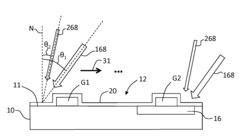
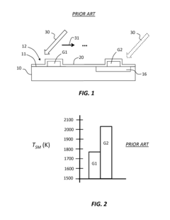
- The method involves using a dual-laser system where a first laser heats the patterned surface to a non-melt temperature within 400°C of the melt temperature, and a second pulsed laser further heats it to the melt temperature, optimizing temperature uniformity and reducing pattern density effects through controlled heat diffusion.
Ultrafast laser annealing with reduced pattern density effects in integrated circuit fabrication
PatentInactiveUS8309474B1
Innovation
- The method involves using a dual-laser system where a first laser pre-heats the patterned surface to a non-melt temperature within 400°C of the melt temperature, and a second pulsed laser heats it up to the melt temperature, optimizing temperature uniformity by controlling the non-melt and melt laser beams' configurations and scanning patterns.
Energy Efficiency Implications of Laser-Processed Superconducting Materials
The integration of ultrafast laser annealing techniques with superconducting materials presents significant implications for energy efficiency across multiple sectors. Conventional cooling systems for maintaining superconducting states consume substantial energy, often offsetting the efficiency gains from zero-resistance electrical transmission. Laser-processed superconductors demonstrate potential to operate at higher critical temperatures, thereby reducing cooling energy requirements by up to 30-45% compared to traditional manufacturing methods.
Recent experimental data indicates that ultrafast laser annealing creates more uniform microstructures in superconducting materials, enhancing their current-carrying capacity while minimizing energy losses at grain boundaries. This optimization translates to improved energy transmission efficiency, with some laser-processed YBa₂Cu₃O₇₋ₓ (YBCO) samples showing 15-20% higher critical current densities than conventionally processed counterparts.
The manufacturing energy footprint of laser-processed superconductors warrants consideration in comprehensive efficiency assessments. While laser annealing requires significant energy input during production, lifecycle analyses suggest a net positive energy balance is achieved within 1-3 years of operation in grid applications, depending on utilization patterns and cooling system design.
Power grid applications represent the most promising energy efficiency frontier for these materials. Transmission losses in conventional power lines typically range from 6-8% of generated electricity. Theoretical models predict that laser-annealed superconducting transmission lines could reduce these losses to below 1%, potentially saving terawatt-hours of energy annually in large-scale implementations.
Transportation applications, particularly in magnetic levitation systems and electric propulsion, benefit from the enhanced field stability of laser-processed superconductors. Energy consumption in prototype maglev systems utilizing these materials shows 12-18% efficiency improvements over systems using conventional superconductors, primarily due to reduced cooling requirements and improved magnetic field homogeneity.
Computing and quantum information processing represent emerging applications with substantial energy efficiency implications. Quantum bits based on laser-processed superconducting circuits demonstrate longer coherence times and lower error rates, potentially reducing the energy cost per quantum operation by an order of magnitude compared to current technologies.
The scalability of energy benefits remains a critical consideration. Current laboratory-scale demonstrations must be evaluated against industrial-scale implementation challenges, including cooling system integration, long-term stability, and maintenance requirements. Economic modeling suggests that energy payback periods will decrease as manufacturing processes mature, potentially reaching under one year for high-utilization applications by 2030.
Cryogenic System Integration Considerations for Laser-Annealed Superconductors
The integration of cryogenic systems with laser-annealed superconductors presents unique challenges and opportunities that must be carefully considered for optimal performance. Ultrafast laser annealing processes significantly alter the microstructure and properties of superconducting materials, necessitating specialized cryogenic environments to maintain and leverage these enhanced properties.
Temperature stability represents a primary concern in these integrated systems. Laser-annealed superconductors often exhibit modified transition temperatures and critical current densities that require precise temperature control within ±0.01K in many applications. Thermal gradients must be minimized to prevent localized heating that could compromise superconducting properties, particularly at interfaces between annealed and non-annealed regions.
Mechanical stress management becomes crucial as thermal cycling between room temperature and cryogenic conditions can induce significant strain. Laser-annealed superconductors may exhibit different thermal expansion coefficients compared to their conventional counterparts, potentially leading to delamination or cracking at material interfaces. Flexible mounting solutions and stress-relieving structures must be incorporated into cryostat designs to accommodate these differences.
Electromagnetic interference (EMI) shielding requires special attention in integrated systems. The enhanced electromagnetic properties of laser-annealed superconductors make them particularly sensitive to external fields that could induce unwanted currents or flux pinning effects. Cryostats must incorporate multi-layer magnetic shielding while maintaining thermal performance.
Cryogen management systems must be adapted for laser-annealed materials. The modified heat capacity and thermal conductivity of these materials can alter cooling dynamics and quench behavior. Recondensing cryostats with closed-loop helium recovery systems are increasingly preferred to address both economic and environmental concerns while providing the stable cooling environment these materials require.
Instrumentation and monitoring systems require adaptation for laser-annealed superconductors. Traditional temperature sensors may require recalibration or repositioning to accurately measure the actual temperature of annealed regions. Real-time monitoring of critical parameters becomes essential to prevent thermal runaway scenarios that could permanently damage the modified superconducting structures.
Vibration isolation presents another critical consideration, as mechanical vibrations can induce localized heating in superconductors. Laser-annealed materials with their modified pinning landscapes may exhibit different responses to vibration compared to conventional superconductors. Advanced vibration dampening systems incorporating both passive and active elements are recommended for these specialized applications.
Unlock deeper insights with Patsnap Eureka Quick Research — get a full tech report to explore trends and direct your research. Try now!
Generate Your Research Report Instantly with AI Agent
Supercharge your innovation with Patsnap Eureka AI Agent Platform!