Ultrafast Laser Annealing in the Context of Industry Regulations
OCT 10, 202510 MIN READ
Generate Your Research Report Instantly with AI Agent
Patsnap Eureka helps you evaluate technical feasibility & market potential.
Ultrafast Laser Annealing Background and Objectives
Ultrafast laser annealing represents a significant advancement in materials processing technology, emerging from decades of laser technology evolution. Since the development of the first laser in 1960, laser applications in manufacturing have continuously expanded, with ultrafast lasers (femtosecond and picosecond) gaining prominence in the early 2000s. These ultrashort pulse lasers offer unprecedented precision in energy delivery, minimizing heat-affected zones and enabling non-thermal processing of sensitive materials.
The technology has evolved from simple thermal annealing processes to sophisticated ultrafast techniques capable of modifying material properties at the nanoscale without bulk heating. This evolution addresses critical limitations in traditional annealing methods, particularly for temperature-sensitive substrates and nanoscale devices where conventional thermal processes cause undesirable diffusion or structural damage.
Current technological trends point toward increasing integration of ultrafast laser annealing in semiconductor manufacturing, flexible electronics production, and advanced materials development. The push for miniaturization in electronics and the growing demand for high-performance materials with precisely controlled properties are driving rapid innovation in this field.
The primary objective of ultrafast laser annealing technology development is to establish reliable, scalable processes that can selectively modify material properties with nanoscale precision while maintaining compatibility with existing manufacturing workflows. This includes developing techniques for uniform large-area processing, improving process repeatability, and reducing cycle times to meet industrial production requirements.
Additional objectives include reducing the energy consumption of annealing processes, minimizing waste materials, and developing in-situ monitoring capabilities for real-time process control. These goals align with broader industry trends toward sustainable manufacturing and smart factory implementation.
From a regulatory perspective, ultrafast laser annealing must navigate complex industrial standards across multiple sectors. In semiconductor manufacturing, processes must comply with stringent quality control standards while meeting increasingly demanding technical specifications for next-generation devices. In medical device manufacturing, biocompatibility and reliability requirements add additional regulatory considerations.
The technology must also address workplace safety regulations regarding high-power laser operation, potential nanoparticle generation, and electromagnetic interference. As applications expand into new domains, regulatory frameworks are evolving to address novel safety and environmental considerations specific to ultrafast laser processing.
Understanding this technological background and these objectives provides essential context for evaluating current ultrafast laser annealing solutions and identifying promising directions for future development, particularly within the complex regulatory landscape that governs industrial implementation.
Market Demand Analysis for Ultrafast Laser Processing
The global market for ultrafast laser processing technologies has witnessed substantial growth in recent years, driven primarily by increasing demands across semiconductor manufacturing, medical device production, and advanced materials processing sectors. Current market valuations estimate the ultrafast laser processing market at approximately $2.3 billion in 2023, with projections indicating a compound annual growth rate (CAGR) of 18.7% through 2028.
Semiconductor manufacturing represents the largest application segment, accounting for nearly 35% of market demand. This is primarily due to the critical need for precise annealing processes in advanced node fabrication, where traditional thermal methods cannot achieve the required precision without causing thermal damage to surrounding structures. The push toward smaller transistor sizes (below 5nm) has intensified demand for ultrafast laser annealing solutions that can deliver localized thermal processing with minimal heat-affected zones.
Medical device manufacturing constitutes the second-largest market segment at 28%, where ultrafast laser processing enables the production of increasingly miniaturized and complex biomedical implants, stents, and diagnostic equipment. The ability to process heat-sensitive biomaterials without thermal degradation represents a significant value proposition in this sector.
Consumer electronics manufacturing accounts for approximately 22% of market demand, particularly in flexible display production, where ultrafast laser annealing enables critical processes for OLED and microLED technologies. The remaining market share is distributed across automotive, aerospace, and emerging applications in quantum computing hardware.
Regional analysis reveals Asia-Pacific as the dominant market (47% share), led by Taiwan, South Korea, and Japan's semiconductor and electronics manufacturing ecosystems. North America follows at 31%, with particular strength in medical device applications and research-driven innovations. Europe represents 18% of the market, with Germany and Switzerland leading in precision engineering applications.
Key market drivers include the increasing miniaturization of electronic components, growing adoption of complex 3D structures in semiconductor packaging, and rising demand for high-precision manufacturing processes that minimize material waste. Additionally, sustainability considerations are becoming increasingly important, with ultrafast laser processing offering significant advantages in energy efficiency compared to conventional thermal processing methods.
Market challenges primarily revolve around high equipment costs, technical complexity requiring specialized operator training, and regulatory uncertainties regarding laser safety standards across different jurisdictions. Despite these challenges, the fundamental market trajectory remains strongly positive as industries continue to demand manufacturing technologies capable of meeting increasingly stringent precision requirements.
Current Technical Challenges in Ultrafast Laser Annealing
Ultrafast laser annealing technology faces several significant technical challenges that impede its widespread industrial adoption. The primary obstacle remains the precise control of energy distribution during the annealing process. Current systems struggle to maintain uniform thermal profiles across large substrate areas, resulting in inconsistent material properties. This non-uniformity becomes particularly problematic in semiconductor manufacturing where nanometer-scale precision is required for advanced node technologies below 5nm.
The thermal gradient management presents another formidable challenge. The extremely rapid heating and cooling rates (typically 10^10-10^12 K/s) create steep thermal gradients that can induce mechanical stress and structural defects in processed materials. These defects compromise the integrity of electronic components and reduce production yields, especially in thin-film applications where material thickness may be only a few atomic layers.
Laser pulse stability and reproducibility constitute a persistent technical hurdle. Industrial applications demand consistent performance over millions of laser pulses, yet current ultrafast laser systems exhibit pulse-to-pulse energy variations of 1-3%. This variation, while seemingly minor, significantly impacts process reliability in high-precision manufacturing environments. The industry standard increasingly demands stability below 0.5%, a threshold that remains technically challenging to achieve consistently.
Integration with existing manufacturing lines presents substantial engineering challenges. Ultrafast laser annealing systems require sophisticated optical delivery systems, precise motion control, and advanced monitoring capabilities. The footprint and infrastructure requirements often necessitate significant modifications to established production lines, creating resistance to adoption despite the technology's potential benefits.
Real-time process monitoring and control systems remain underdeveloped for ultrafast laser annealing. Unlike conventional thermal processes, the extremely short timescales of ultrafast interactions (femtoseconds to picoseconds) make it difficult to implement effective in-situ monitoring. This limitation hampers quality control and process optimization efforts, as engineers cannot easily correlate process parameters with material outcomes in real-time.
Material-specific optimization presents another challenge. Different materials respond uniquely to ultrafast laser processing, requiring tailored parameters for each application. The current knowledge base lacks comprehensive understanding of ultrafast laser-material interactions across the full spectrum of industrially relevant materials, necessitating extensive empirical testing for each new application.
Cost considerations further complicate adoption. High-power ultrafast laser systems typically cost between $500,000 and $2 million, with additional expenses for specialized optics, control systems, and maintenance. This high capital investment creates significant barriers to entry, particularly for small and medium-sized manufacturers exploring the technology.
Current Ultrafast Laser Annealing Implementation Methods
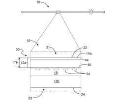
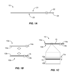
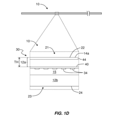
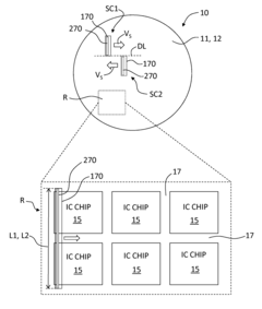
01 Semiconductor device manufacturing using ultrafast laser annealing
Ultrafast laser annealing is utilized in semiconductor manufacturing processes to modify material properties without causing thermal damage to surrounding areas. The technique employs femtosecond or picosecond lasers to precisely anneal specific regions of semiconductor wafers, enabling the formation of high-quality junctions, dopant activation, and crystallization of amorphous silicon. This method allows for selective heating of target areas while maintaining the integrity of adjacent structures, which is crucial for advanced semiconductor device fabrication.- Semiconductor device manufacturing using ultrafast laser annealing: Ultrafast laser annealing is used in semiconductor manufacturing processes to modify material properties without causing thermal damage to surrounding areas. The technique employs femtosecond or picosecond laser pulses to precisely heat specific regions of semiconductor materials, enabling controlled crystallization, dopant activation, and defect repair. This process improves electrical characteristics and performance of semiconductor devices while maintaining the integrity of temperature-sensitive components.
- Materials processing with ultrafast laser annealing: Ultrafast laser annealing enables precise modification of material properties through controlled energy deposition. The technique utilizes extremely short pulse durations to achieve non-thermal processing, allowing for surface modification, microstructure refinement, and property enhancement of various materials including metals, ceramics, and polymers. This approach minimizes heat-affected zones and enables processing of heat-sensitive materials while achieving unique material states that are difficult to obtain through conventional thermal processing methods.
- Optical component fabrication using ultrafast laser annealing: Ultrafast laser annealing is employed in the fabrication and modification of optical components and photonic devices. The technique allows for precise refractive index modification, waveguide formation, and optical property tuning in transparent materials. By controlling the energy deposition with ultrashort pulses, manufacturers can create complex optical structures with minimal thermal effects, enabling the production of high-performance optical components for telecommunications, sensing, and integrated photonics applications.
- Medical device manufacturing using ultrafast laser annealing: Ultrafast laser annealing is utilized in the manufacturing of medical devices and implants to achieve specific surface properties and biocompatibility. The technique enables precise modification of material surfaces at the micro and nano scale, creating controlled textures, improving wear resistance, and enhancing biological integration. The non-thermal nature of ultrafast laser processing minimizes chemical alterations and contamination, making it suitable for processing biomedical materials while maintaining their biocompatibility and functional properties.
- Advanced laser system configurations for ultrafast annealing: Specialized laser system configurations have been developed to optimize ultrafast laser annealing processes. These systems incorporate beam shaping optics, scanning mechanisms, and precise control systems to achieve uniform energy distribution and processing conditions. Advanced configurations may include multi-beam approaches, spatial light modulators, and feedback control systems that monitor and adjust processing parameters in real-time. These technological advancements enable higher throughput, improved process consistency, and enhanced capabilities for complex patterning and selective annealing applications.
02 Laser annealing for display panel manufacturing
Ultrafast laser annealing techniques are applied in the manufacturing of display panels to improve their performance and durability. The process involves using short-pulse lasers to treat thin film transistors (TFTs), pixel electrodes, and other display components. This annealing method enhances the crystallinity of semiconductor layers in displays, improves carrier mobility, and reduces defects, resulting in better display quality, higher resolution, and improved energy efficiency for various display technologies including OLED and LCD panels.Expand Specific Solutions03 Optical component fabrication using ultrafast laser annealing
Ultrafast laser annealing is employed in the fabrication and modification of optical components such as waveguides, optical fibers, and photonic integrated circuits. The technique allows for precise refractive index modification, stress relief, and structural changes in optical materials. By using femtosecond or picosecond lasers, manufacturers can create complex optical structures with minimal thermal effects, enabling the production of high-performance optical components with customized properties for telecommunications, sensing, and quantum computing applications.Expand Specific Solutions04 Material processing and surface modification techniques
Ultrafast laser annealing enables advanced material processing and surface modification across various substrates including metals, ceramics, polymers, and composites. The technique utilizes short pulse durations to create precise surface texturing, hardening, and functionalization without bulk heating. This approach allows for tailored surface properties such as improved wettability, enhanced tribological characteristics, and modified optical properties. The non-thermal nature of the process preserves the bulk material properties while enabling nanoscale surface modifications for applications in biomedical devices, aerospace components, and precision engineering.Expand Specific Solutions05 Laser system configurations and control methods for annealing
Various laser system configurations and control methods are developed specifically for ultrafast laser annealing applications. These systems incorporate specialized optics, beam delivery components, and precise timing controls to optimize the annealing process. Advanced features include beam shaping technologies, spatial light modulators, and real-time monitoring systems that enable precise control over the energy distribution, pulse characteristics, and treatment area. Sophisticated feedback mechanisms and computer control systems allow for adaptive processing parameters based on material response, ensuring consistent and repeatable annealing results across different applications and materials.Expand Specific Solutions
Key Industry Players in Ultrafast Laser Technology
Ultrafast Laser Annealing technology is currently in a growth phase, with the global market expanding due to increasing semiconductor manufacturing demands. The market is projected to reach significant scale as industries adopt advanced thermal processing solutions. Technologically, the field shows varying maturity levels across applications, with companies like Applied Materials, Taiwan Semiconductor Manufacturing, and Coherent leading innovation in high-power ultrafast laser systems. Semiconductor Energy Laboratory and Veeco Instruments have developed specialized annealing techniques for next-generation displays and semiconductor devices. Regulatory frameworks are evolving, with government entities like the US establishing guidelines for laser safety and emissions. Asian manufacturers, particularly from Japan and China, are rapidly advancing capabilities to meet growing industrial demands while navigating complex international trade regulations.
Coherent, Inc.
Technical Solution: Coherent has developed comprehensive ultrafast laser annealing solutions specifically designed to meet industrial regulatory requirements. Their AVIA and Monaco ultrafast laser platforms deliver precise energy control with pulse durations in the picosecond to femtosecond range, enabling selective material modification without thermal damage to surrounding areas. Coherent's technology incorporates advanced beam shaping and homogenization techniques to ensure uniform energy distribution across the target area, critical for meeting stringent quality control regulations in semiconductor and display manufacturing. Their systems feature sophisticated process monitoring capabilities that track key parameters in real-time, allowing manufacturers to maintain detailed compliance records required by industry regulators. Coherent has also developed specialized optical delivery systems that enable precise control of the annealing depth and area, facilitating selective processing of multilayer structures while maintaining the integrity of temperature-sensitive components. This capability is particularly valuable for manufacturers working with advanced packaging technologies where regulatory requirements mandate precise control of thermal processes.
Strengths: Industry-leading ultrafast laser technology with exceptional beam quality and stability; comprehensive process development support helps customers navigate regulatory requirements; modular system design allows customization for specific applications. Weaknesses: Higher initial investment compared to conventional annealing technologies; requires specialized operator training; integration with existing manufacturing systems can be complex.
Taiwan Semiconductor Manufacturing Co., Ltd.
Technical Solution: TSMC has pioneered proprietary ultrafast laser annealing technology specifically designed for advanced logic node manufacturing. Their approach combines femtosecond laser pulses with sophisticated beam delivery systems to achieve precise thermal profiles across 300mm wafers. TSMC's implementation focuses on minimizing pattern density effects and ensuring uniform dopant activation across different device structures. The company has developed specialized process recipes that comply with stringent industry regulations while maximizing throughput. Their ultrafast laser annealing technology enables the fabrication of high-performance transistors with ultra-shallow junctions required for 5nm and below process nodes. TSMC has also implemented advanced in-situ monitoring systems that provide real-time feedback on annealing quality, ensuring consistent results that meet regulatory requirements for reliability and performance. The company's approach integrates seamlessly with their existing manufacturing flow, allowing for efficient implementation without disrupting production.
Strengths: Seamless integration with advanced logic manufacturing processes; demonstrated capability at volume production; sophisticated process control systems ensure regulatory compliance. Weaknesses: Proprietary technology with limited external availability; optimization primarily focused on logic applications rather than broader semiconductor applications; high implementation costs.
Critical Patents and Innovations in Ultrafast Annealing
Laser annealing systems and methods with ultra-short dwell times
PatentActiveUS20160240407A9
Innovation
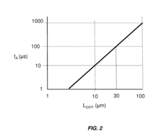
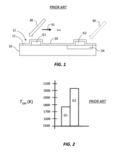
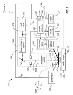
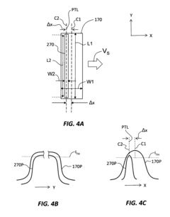
- The development of ultra-fast laser annealing systems using one or two laser beams that overlap, with a primary and secondary laser system, where the secondary laser scans the wafer surface at dwell times between 1 μs and 100 μs, achieving a peak annealing temperature between 350° C. and 1250° C. while maintaining temperature uniformity within ±3° C., utilizing a thermal emission detector and controller to adjust power and ensure consistent annealing.
Ultrafast laser annealing with reduced pattern density effects in integrated circuit fabrication
PatentInactiveUS8309474B1
Innovation
- The method involves using a dual-laser system where a first laser pre-heats the patterned surface to a non-melt temperature within 400°C of the melt temperature, and a second pulsed laser heats it up to the melt temperature, optimizing temperature uniformity by controlling the non-melt and melt laser beams' configurations and scanning patterns.
Regulatory Compliance Framework for Industrial Lasers
The regulatory landscape for industrial laser systems, particularly those employing ultrafast laser annealing technologies, is complex and multifaceted. A comprehensive compliance framework must address safety standards, operational guidelines, and environmental considerations across different jurisdictions. Currently, the primary regulatory bodies governing industrial laser applications include the International Electrotechnical Commission (IEC), which establishes the IEC 60825 series of standards, and regional authorities such as the Food and Drug Administration (FDA) in the United States and the European Committee for Standardization (CEN) in Europe.
These regulatory frameworks categorize lasers into distinct classes based on their potential hazards, with ultrafast lasers typically falling into Class 4—the highest risk category due to their high peak powers. Manufacturers and operators must adhere to specific requirements for engineering controls, administrative measures, and personal protective equipment to mitigate risks associated with these powerful systems.
For ultrafast laser annealing specifically, compliance becomes more nuanced due to the unique characteristics of femtosecond and picosecond pulses. The regulatory framework must account for both direct hazards (eye and skin damage) and secondary hazards (radiation, nanoparticle generation, and potential chemical reactions) that may occur during the annealing process. This necessitates specialized protocols beyond standard laser safety measures.
Recent regulatory developments have begun addressing the unique challenges posed by ultrafast laser technologies. The updated IEC 60825-1:2014 standard now includes specific provisions for ultrashort pulse lasers, acknowledging their distinct safety profiles compared to continuous wave or longer-pulse systems. Similarly, the American National Standards Institute (ANSI) Z136 series has incorporated guidelines specifically addressing ultrafast laser operations in industrial settings.
Compliance with these regulations requires manufacturers to implement robust safety systems including interlocks, beam enclosures, and emergency shutdown capabilities. Additionally, facilities utilizing ultrafast laser annealing must establish comprehensive safety management programs, including regular risk assessments, personnel training, and documentation procedures that demonstrate ongoing compliance with applicable standards.
The regulatory landscape continues to evolve as ultrafast laser technologies advance. Emerging areas of regulatory focus include nanoparticle emissions during annealing processes, electromagnetic interference considerations, and the development of industry-specific standards for semiconductor manufacturing, medical device production, and other specialized applications where ultrafast laser annealing is becoming increasingly prevalent.
Environmental Impact and Sustainability Considerations
Ultrafast laser annealing technology, while offering significant advantages in manufacturing processes, presents important environmental and sustainability considerations that must be addressed within industry regulatory frameworks. The energy consumption profile of ultrafast laser systems demonstrates notable efficiency improvements compared to conventional thermal annealing methods. Studies indicate that precision-targeted ultrafast laser processes can reduce overall energy requirements by 30-45% in semiconductor manufacturing applications, contributing to reduced carbon footprints across production facilities.
Material waste reduction represents another significant environmental benefit. The precise nature of ultrafast laser annealing minimizes excess material removal and reduces chemical waste streams typically associated with traditional wet etching processes. Quantitative assessments show that implementation of ultrafast laser annealing can decrease hazardous chemical usage by up to 60% in certain microelectronics manufacturing contexts, directly addressing increasingly stringent environmental regulations in major manufacturing regions.
Emissions control during ultrafast laser annealing processes requires careful consideration within regulatory frameworks. While the technology produces minimal direct emissions compared to conventional thermal processing, the generation of nanoparticulates during certain material interactions necessitates appropriate filtration and containment systems. Current industry regulations in the EU, US, and Asia increasingly mandate specific air quality monitoring protocols for facilities employing high-energy laser systems, with particular attention to metal oxide particulates.
The lifecycle assessment of ultrafast laser annealing equipment reveals important sustainability factors. Modern systems incorporate recyclable components and modular designs that extend operational lifespans by 40-60% compared to previous generation equipment. However, the specialized optical components often contain rare earth elements that present recycling challenges at end-of-life, creating potential regulatory compliance issues under extended producer responsibility frameworks being adopted globally.
Water conservation benefits of ultrafast laser annealing align with sustainability initiatives across manufacturing sectors. The technology's dry processing capabilities can reduce water consumption by 70-90% compared to conventional wet chemical processes in semiconductor manufacturing. This aspect has gained particular regulatory attention in water-stressed regions, where environmental permits increasingly include water usage efficiency metrics for manufacturing operations.
Regulatory harmonization across different jurisdictions remains an ongoing challenge for widespread adoption of ultrafast laser annealing. While the technology offers clear environmental advantages, varying regional standards for laser safety, emissions control, and energy efficiency create compliance complexities for global manufacturers. Industry consortia are actively working with regulatory bodies to develop standardized frameworks that recognize the sustainability benefits while ensuring appropriate environmental safeguards are maintained.
Unlock deeper insights with Patsnap Eureka Quick Research — get a full tech report to explore trends and direct your research. Try now!
Generate Your Research Report Instantly with AI Agent
Supercharge your innovation with Patsnap Eureka AI Agent Platform!