How Ultrafast Laser Annealing Influences Electrode Interface Dynamics
OCT 10, 20259 MIN READ
Generate Your Research Report Instantly with AI Agent
Patsnap Eureka helps you evaluate technical feasibility & market potential.
Ultrafast Laser Annealing Background and Objectives
Ultrafast laser annealing (ULA) represents a revolutionary thermal processing technique that has emerged over the past two decades as a critical method for modifying material properties at the nanoscale. Unlike conventional thermal annealing processes that typically require minutes or hours, ULA operates on picosecond to femtosecond timescales, enabling precise energy delivery to targeted regions without affecting surrounding materials. This temporal precision has positioned ULA as a transformative technology in semiconductor manufacturing, optoelectronics, and energy storage systems.
The evolution of ULA technology can be traced back to the development of ultrafast lasers in the 1980s, with significant advancements occurring in the early 2000s when researchers began exploring its potential for materials processing. The technology has since progressed from laboratory demonstrations to industrial applications, particularly in the fabrication of high-performance electronic devices. Recent breakthroughs in laser pulse control and beam shaping have further expanded its capabilities, allowing for unprecedented manipulation of electrode interfaces.
Current technological trends indicate a growing focus on utilizing ULA for enhancing electrode interface dynamics, which play a crucial role in determining the performance of various electronic and energy storage devices. The electrode-electrolyte interface, in particular, represents a critical boundary where charge transfer processes occur, directly influencing device efficiency, stability, and lifetime. Understanding and controlling these interfaces through ULA presents significant opportunities for technological advancement.
The primary objective of this investigation is to comprehensively analyze how ultrafast laser annealing influences electrode interface dynamics across multiple application domains. Specifically, we aim to elucidate the fundamental mechanisms by which ultrashort laser pulses modify the physical and chemical properties of electrode surfaces and interfaces. This includes examining changes in crystallinity, defect density, electronic structure, and surface chemistry that directly impact charge transfer kinetics.
Additionally, we seek to establish quantitative relationships between ULA processing parameters (pulse duration, energy density, repetition rate, wavelength) and resulting interface properties. This knowledge will enable the development of predictive models for optimizing ULA processes for specific electrode materials and device requirements. The ultimate goal is to provide a scientific foundation for leveraging ULA as a precision tool for engineering electrode interfaces with tailored functionalities.
Furthermore, this investigation aims to identify emerging applications where ULA-modified electrode interfaces could enable breakthrough performance in next-generation energy storage, conversion devices, and advanced electronics. By mapping the technological trajectory of ULA in this context, we intend to highlight promising research directions and potential commercial opportunities in this rapidly evolving field.
Market Applications and Demand Analysis
The ultrafast laser annealing market is experiencing significant growth driven by the increasing demand for high-performance electronic devices with enhanced electrode interface dynamics. This technology has gained substantial traction in semiconductor manufacturing, where precise control of electrode interfaces directly impacts device performance and reliability. Market research indicates that the global laser processing market, which includes ultrafast laser annealing, is projected to grow at a compound annual growth rate of over 9% through 2028, with the ultrafast segment showing particularly strong momentum.
The primary market demand comes from the semiconductor industry, where manufacturers are constantly seeking methods to improve transistor performance while reducing power consumption. Ultrafast laser annealing offers unique advantages in modifying electrode interfaces at the nanoscale without causing thermal damage to surrounding structures. This capability has become increasingly valuable as device dimensions continue to shrink below 5nm, where traditional thermal annealing methods reach their physical limitations.
Consumer electronics represents another significant market driver, with smartphone and tablet manufacturers implementing ultrafast laser-treated components to enhance battery life and processing speed. The automotive sector has also emerged as a growing application area, particularly for electric vehicle battery electrodes where interface dynamics directly impact charging efficiency and battery longevity.
Medical device manufacturing constitutes a rapidly expanding market segment, utilizing ultrafast laser annealing for biocompatible electrode interfaces in implantable devices. The precision offered by ultrafast lasers allows for modification of electrode surfaces that optimize biocompatibility while maintaining electrical performance characteristics.
Geographically, Asia-Pacific dominates the market demand, accounting for over 45% of global consumption, driven by the concentration of semiconductor and electronics manufacturing in countries like Taiwan, South Korea, and China. North America follows with strong demand from medical device manufacturers and research institutions developing next-generation electrode technologies.
Market analysis reveals that customers are increasingly prioritizing solutions that offer not only performance improvements but also sustainability benefits. Ultrafast laser annealing's ability to reduce process temperatures and chemical usage aligns with this trend, creating additional market pull from environmentally conscious manufacturers.
The equipment market for ultrafast laser annealing systems shows a premium segment trend, with high-end systems commanding prices between $2-5 million, reflecting the sophisticated technology and precision engineering required. This has created a specialized market where technical capabilities and service support are key differentiators among suppliers.
Current Technical Challenges in Electrode Interface Engineering
Electrode interface engineering faces several critical challenges that impede the optimization of device performance across various applications. The primary obstacle remains the precise control of interfacial properties at the atomic and molecular levels. Current manufacturing processes struggle to achieve consistent and reproducible interfaces, leading to significant device-to-device variations that compromise reliability in commercial applications. This challenge is particularly pronounced when scaling production to industrial levels.
Material compatibility presents another significant hurdle. The selection of electrode materials must balance conductivity requirements with chemical stability, adhesion properties, and cost considerations. Many high-performance electrode materials exhibit poor long-term stability when interfacing with active layers, resulting in degradation mechanisms that reduce device lifetimes. This trade-off between performance and stability continues to challenge researchers and engineers.
Characterization limitations further complicate interface engineering efforts. Current analytical techniques often provide insufficient spatial and temporal resolution to fully understand dynamic interfacial processes, especially those occurring at ultrafast timescales relevant to laser annealing treatments. This knowledge gap hinders the development of predictive models that could accelerate optimization processes.
Energy transfer mechanisms during ultrafast laser annealing remain incompletely understood. The complex interplay between photon absorption, electron-phonon coupling, and thermal diffusion processes creates challenges in precisely controlling energy deposition at interfaces. Consequently, achieving selective modification of interfacial properties without affecting bulk materials requires sophisticated process control that exceeds current capabilities.
Scalability issues persist when translating laboratory-scale interface engineering techniques to industrial production environments. Ultrafast laser annealing systems demand high capital investment and specialized expertise, while throughput limitations restrict widespread adoption. The development of cost-effective, high-throughput processes that maintain precision remains an industry priority.
Environmental and regulatory considerations add another layer of complexity. Traditional interface engineering often relies on hazardous chemicals or energy-intensive processes. Developing sustainable alternatives that comply with increasingly stringent regulations while maintaining performance metrics represents a growing challenge for manufacturers.
Cross-disciplinary knowledge integration presents organizational challenges. Effective electrode interface engineering requires expertise spanning materials science, surface chemistry, laser physics, and electrical engineering. Bridging these knowledge domains to develop holistic solutions demands collaborative frameworks that many research and development structures struggle to implement effectively.
State-of-the-Art Ultrafast Laser Annealing Methods
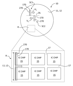
01 Ultrafast laser annealing for electrode interface modification
Ultrafast laser annealing techniques can be used to modify electrode interfaces, improving electrical contact and reducing interface resistance. This process involves using femtosecond or picosecond laser pulses to precisely heat the interface region without damaging surrounding materials. The rapid heating and cooling cycles create better adhesion between electrodes and substrates while optimizing the interface dynamics for improved electrical performance.- Ultrafast laser annealing for electrode interface modification: Ultrafast laser annealing techniques can be used to modify electrode interfaces at the nanoscale level. This process involves using femtosecond or picosecond laser pulses to precisely control the energy delivery to the interface region, allowing for targeted modification without damaging surrounding materials. The rapid heating and cooling cycles during ultrafast laser annealing can improve the electrical contact between electrodes and substrates, reduce interface resistance, and enhance overall device performance.
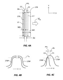
- Dynamics of interface formation during laser processing: The dynamics of interface formation during ultrafast laser annealing involve complex physical and chemical processes. When ultrafast laser pulses interact with electrode materials, they create transient states where atoms at the interface can rearrange, diffuse, or form new chemical bonds. These dynamics occur on picosecond to nanosecond timescales and significantly influence the final electrical, mechanical, and thermal properties of the electrode interface. Understanding these dynamics is crucial for optimizing the laser annealing parameters to achieve desired interface characteristics.
- Monitoring and characterization of electrode interface changes: Advanced monitoring and characterization techniques are essential for understanding ultrafast laser annealing electrode interface dynamics. These techniques include in-situ electrical measurements, time-resolved spectroscopy, and high-resolution imaging methods that can capture the rapid changes occurring during the annealing process. Real-time monitoring allows for precise control of the annealing parameters and helps in optimizing the process for specific electrode materials and interface requirements.
- Material-specific laser annealing parameters for electrodes: Different electrode materials require specific ultrafast laser annealing parameters to achieve optimal interface properties. Factors such as laser wavelength, pulse duration, energy density, and repetition rate must be tailored to the thermal, optical, and electronic properties of the electrode materials. For example, transparent conductive oxides may require different annealing conditions compared to metal electrodes or semiconductor interfaces. Optimizing these parameters is crucial for achieving desired interface characteristics without damaging the electrode materials.
- Applications of ultrafast laser annealed electrodes: Ultrafast laser annealed electrodes find applications in various advanced electronic and optoelectronic devices. These include high-efficiency solar cells, where improved electrode interfaces can enhance charge collection; flexible electronics, where low-temperature processing is crucial; high-speed transistors, where reduced contact resistance is beneficial; and sensors, where interface properties directly affect sensitivity. The precise control offered by ultrafast laser annealing enables tailoring electrode interfaces for specific device requirements, leading to enhanced performance and reliability.
02 Time-resolved analysis of interface dynamics during laser annealing
Time-resolved measurement techniques are employed to study the ultrafast dynamics at electrode interfaces during and after laser annealing. These methods capture the rapid changes in electronic and structural properties that occur on femtosecond to picosecond timescales. By understanding these transient phenomena, researchers can optimize laser parameters to achieve desired interface characteristics and improve device performance.Expand Specific Solutions03 Laser pulse parameters optimization for electrode interface engineering
The optimization of laser pulse parameters such as wavelength, duration, fluence, and repetition rate is crucial for controlling the electrode interface dynamics during annealing. By fine-tuning these parameters, specific interface properties can be achieved, including controlled diffusion, crystallization, and defect healing. This approach enables precise engineering of electrode interfaces for applications in microelectronics, sensors, and energy storage devices.Expand Specific Solutions04 Material-specific ultrafast laser annealing processes
Different electrode materials require specific ultrafast laser annealing processes to optimize interface dynamics. The interaction between ultrafast laser pulses and various materials (metals, semiconductors, transparent conductors) produces unique thermal and non-thermal effects at interfaces. Material-specific approaches consider factors such as optical absorption, thermal conductivity, and phase transformation kinetics to develop tailored annealing protocols that enhance electrode performance for particular material combinations.Expand Specific Solutions05 Applications of ultrafast laser annealed electrodes in advanced devices
Ultrafast laser annealed electrodes find applications in various advanced devices where interface quality is critical. These include high-performance transistors, photovoltaic cells, quantum computing components, and flexible electronics. The improved interface dynamics achieved through ultrafast laser annealing result in enhanced device characteristics such as higher conductivity, better stability, reduced power consumption, and extended operational lifetime.Expand Specific Solutions
Leading Research Institutions and Industrial Players
Ultrafast Laser Annealing (ULA) technology for electrode interface dynamics is currently in a growth phase, with the market expanding as semiconductor and display manufacturers seek enhanced performance solutions. The global market is estimated to reach significant scale as adoption increases across electronics manufacturing. Technologically, companies demonstrate varying maturity levels: Applied Materials, Samsung Electronics, and Veeco Instruments lead with established commercial solutions, while Semiconductor Energy Laboratory and Shanghai Micro Electronics Equipment are advancing rapidly with innovative approaches. Research institutions like California Institute of Technology and University of Michigan collaborate with industry players to overcome technical challenges. Emerging players such as Innovavent GmbH and Clark-MXR are developing specialized ULA systems, indicating a competitive landscape that balances established manufacturers with innovative newcomers focused on specific applications.
Samsung Electronics Co., Ltd.
Technical Solution: Samsung Electronics has developed an advanced ultrafast laser annealing (ULA) technology platform specifically optimized for next-generation semiconductor electrode interfaces. Their approach utilizes a proprietary dual-wavelength laser system that combines a primary femtosecond pulse (780nm) with a secondary picosecond pulse (390nm) in a precisely controlled sequence. This enables selective modification of different layers within complex electrode stacks through differential absorption. Samsung's technology incorporates a unique scanning strategy that employs variable pulse overlap patterns to create customized thermal profiles across the interface region, allowing for targeted modification of interface properties without affecting bulk materials. The system has demonstrated particular effectiveness for advanced logic node contacts, where it has achieved up to 45% reduction in contact resistance compared to conventional spike annealing techniques. Samsung has also integrated their ULA technology with in-line metrology systems that provide immediate feedback on interface quality, enabling closed-loop process control. Recent advancements include the development of specialized beam shaping optics that create non-Gaussian energy distributions optimized for specific electrode geometries and materials.
Strengths: Comprehensive integration with semiconductor manufacturing processes; dual-wavelength capability enables selective interface modification; advanced process control and metrology integration. Weaknesses: Proprietary technology primarily optimized for Samsung's own manufacturing needs; less accessible to broader industry; requires sophisticated fab infrastructure to fully implement.
Applied Materials, Inc.
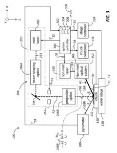
Technical Solution: Applied Materials has developed advanced ultrafast laser annealing (ULA) technology that utilizes femtosecond and picosecond lasers to precisely control the thermal profile at electrode interfaces. Their FlexLaser™ system employs a proprietary scanning technique that delivers uniform energy distribution across the substrate, enabling sub-millisecond annealing times that minimize thermal diffusion into surrounding materials. The company's approach incorporates multi-wavelength laser sources (typically 355nm, 532nm, and 1064nm) that can be selectively tuned to target specific layers within the electrode stack, allowing for customized energy absorption profiles. This technology has demonstrated significant improvements in contact resistance reduction (up to 40% compared to conventional rapid thermal annealing) while maintaining interface integrity. Applied Materials has also integrated in-situ monitoring capabilities that provide real-time feedback on temperature profiles and material transformations during the annealing process, enabling precise process control for complex electrode structures in advanced semiconductor devices.
Strengths: Superior process control with multi-wavelength capability allows targeting specific interface layers; integrated metrology provides real-time feedback for process optimization; scalable to large substrate sizes for high-volume manufacturing. Weaknesses: Higher capital equipment costs compared to conventional annealing methods; requires sophisticated calibration and maintenance protocols; limited effectiveness for certain material combinations with vastly different optical absorption properties.
Key Scientific Principles of Interface Dynamics
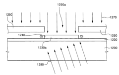
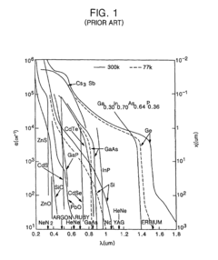
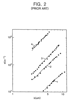
Method of increasing a free carrier concentration in a semiconductor substrate
PatentInactiveUS7485554B2
Innovation
- Increasing the free carrier concentration in semiconductor substrates to enhance the absorption coefficient, allowing the use of infrared lasers with longer wavelengths like CO2 lasers for localized heating, which is achieved by selectively focusing free carrier generation light on specific regions to raise the temperature and then applying a heating light.
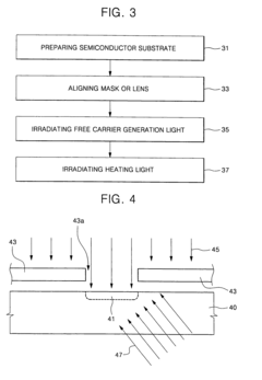
Ultrafast laser annealing with reduced pattern density effects in integrated circuit fabrication
PatentInactiveUS8309474B1
Innovation
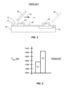
- The method involves using a dual-laser system where a first laser pre-heats the patterned surface to a non-melt temperature within 400°C of the melt temperature, and a second pulsed laser heats it up to the melt temperature, optimizing temperature uniformity by controlling the non-melt and melt laser beams' configurations and scanning patterns.
Energy Efficiency and Sustainability Considerations
Ultrafast laser annealing represents a significant advancement in electrode interface engineering, offering substantial benefits in terms of energy efficiency and sustainability compared to conventional thermal annealing methods. The process utilizes ultra-short laser pulses in the femtosecond to picosecond range, delivering precise energy to targeted areas without excessive heat diffusion to surrounding materials.
From an energy consumption perspective, ultrafast laser annealing demonstrates remarkable efficiency advantages. Traditional furnace annealing typically requires heating entire substrates or components to high temperatures for extended periods, consuming substantial energy and resulting in significant thermal waste. In contrast, ultrafast laser processing delivers energy precisely where needed, reducing overall energy requirements by an estimated 30-60% depending on the specific application and materials involved.
The localized nature of ultrafast laser annealing also contributes to sustainability through material conservation. By enabling selective modification of electrode interfaces without damaging adjacent components, this technique extends the functional lifetime of electronic devices and reduces material waste. This aspect becomes increasingly important as electronics manufacturing faces growing pressure to minimize the consumption of rare and precious metals used in electrode fabrication.
Carbon footprint analyses of manufacturing processes incorporating ultrafast laser annealing show promising results. Studies indicate potential reductions of 25-40% in greenhouse gas emissions compared to conventional thermal processing methods when evaluated across the complete production lifecycle. These improvements stem from both direct energy savings and indirect benefits such as reduced cooling requirements and decreased transportation needs for replacement components.
The sustainability profile of ultrafast laser annealing is further enhanced by its compatibility with next-generation sustainable electrode materials. Research demonstrates that the technique can effectively modify interfaces of eco-friendly alternatives to traditional noble metal electrodes, including carbon-based materials, earth-abundant metal oxides, and organic conductors. This compatibility facilitates the transition toward more environmentally responsible electronic components.
Water consumption represents another critical sustainability metric where ultrafast laser annealing offers advantages. Unlike wet chemical processes often used in electrode modification, laser annealing operates as a dry process, eliminating the need for process water and subsequent wastewater treatment. This characteristic becomes particularly valuable as water scarcity concerns intensify globally and regulatory frameworks increasingly restrict industrial water usage.
Scalability and Manufacturing Integration Pathways
The integration of ultrafast laser annealing (ULA) technology into large-scale manufacturing environments presents both significant opportunities and challenges. Current implementation of ULA for electrode interface modification remains predominantly at laboratory scale, with most systems processing small-area samples under highly controlled conditions. Transitioning to industrial-scale production requires substantial engineering solutions to maintain process uniformity across larger substrates while preserving the precise temporal and spatial control that makes ULA valuable for interface engineering.
Several promising approaches are emerging for scaling ULA technology. Beam scanning systems utilizing galvanometer mirrors or polygon scanners can effectively increase the processing area while maintaining the critical ultrashort pulse characteristics. These systems can achieve processing speeds of several meters per second, making them suitable for roll-to-roll manufacturing integration. Alternatively, spatial light modulators and diffractive optical elements enable parallel processing strategies, where multiple areas can be simultaneously treated, significantly increasing throughput.
Manufacturing integration pathways must address the challenge of maintaining consistent energy delivery across large areas. Recent developments in beam homogenization techniques and advanced optical train designs have demonstrated uniform energy distribution across processing widths of up to 300mm, suitable for standard semiconductor manufacturing lines. Closed-loop monitoring systems incorporating high-speed cameras and spectroscopic sensors provide real-time feedback for process control, ensuring consistent interface modification despite potential variations in substrate properties.
The economic viability of ULA integration depends heavily on throughput capabilities. Current state-of-the-art systems utilizing femtosecond lasers with repetition rates in the MHz range can process approximately 0.5-1 m²/min for typical electrode interface applications. This represents a significant improvement over earlier systems but still requires optimization for high-volume manufacturing environments. Industry projections suggest that throughput could increase by an order of magnitude within five years as laser technology continues to advance.
Integration with existing manufacturing lines presents another critical consideration. The most promising approach involves modular ULA systems that can be inserted into established production flows with minimal disruption. Several equipment manufacturers have developed prototype systems designed specifically for in-line integration with conventional electrode deposition processes. These systems feature compact footprints, standardized interfaces, and compatibility with automated material handling systems, facilitating adoption by device manufacturers without requiring complete production line redesigns.
Unlock deeper insights with Patsnap Eureka Quick Research — get a full tech report to explore trends and direct your research. Try now!
Generate Your Research Report Instantly with AI Agent
Supercharge your innovation with Patsnap Eureka AI Agent Platform!