Crossbar Array Design Optimizations For Scalable In-Memory Computing Systems
SEP 2, 20259 MIN READ
Generate Your Research Report Instantly with AI Agent
Patsnap Eureka helps you evaluate technical feasibility & market potential.
Crossbar Array Technology Evolution and Objectives
Crossbar array technology has evolved significantly over the past two decades, transitioning from a theoretical concept to a practical implementation for in-memory computing systems. Initially developed as a simple grid-like structure for memory applications, crossbar arrays have now become a cornerstone technology for neuromorphic computing, resistive memory, and computational memory architectures.
The evolution began with passive crossbar arrays in the early 2000s, which suffered from sneak path currents and high parasitic resistance. This led to the development of 1T1R (one transistor, one resistor) and 1D1R (one diode, one resistor) architectures to mitigate these issues. By 2010, researchers had demonstrated functional crossbar arrays with memristive elements, enabling analog computation capabilities that closely mimic biological neural networks.
Recent advancements have focused on material innovations, with transition metal oxides, phase change materials, and ferroelectric materials emerging as promising candidates for crossbar array elements. These materials offer improved switching characteristics, retention time, and energy efficiency compared to earlier implementations.
The scaling trajectory has been remarkable, progressing from arrays with hundreds of elements to current demonstrations featuring millions of crosspoints. This scaling has been enabled by advances in fabrication techniques, including atomic layer deposition and precise etching methods that allow for sub-10nm feature sizes.
The primary objectives for crossbar array technology development are multifaceted. First, there is a critical need to improve density scaling while maintaining reliable operation, targeting arrays with billions of crosspoints to support large-scale neural network implementations. Second, reducing energy consumption per operation to sub-femtojoule levels is essential for practical edge computing applications.
Another key objective is enhancing the precision and reliability of analog computing operations within crossbar structures. Current implementations often suffer from device-to-device variability and temporal drift, limiting computational accuracy. Researchers aim to achieve at least 8-bit equivalent precision in analog operations to support modern deep learning workloads.
Additionally, there is a growing focus on developing 3D crossbar architectures to further increase density and reduce interconnect delays. These structures promise to overcome the physical limitations of 2D arrays while introducing new challenges in thermal management and fabrication complexity.
The ultimate goal is to create scalable in-memory computing systems that can deliver orders of magnitude improvements in energy efficiency and computational density compared to conventional von Neumann architectures, particularly for data-intensive applications like artificial intelligence and big data analytics.
Market Analysis for In-Memory Computing Solutions
The in-memory computing (IMC) market is experiencing rapid growth, driven by increasing demands for real-time data processing and the limitations of traditional von Neumann architectures. Current market valuations place the global IMC sector at approximately $3.8 billion in 2023, with projections indicating a compound annual growth rate (CAGR) of 18.5% through 2028, potentially reaching $8.9 billion. This growth trajectory is primarily fueled by applications in artificial intelligence, machine learning, and big data analytics where computational speed and energy efficiency are paramount concerns.
Several key market segments are emerging within the IMC landscape. The enterprise data processing sector currently represents the largest market share at 42%, followed by scientific computing at 28%, and consumer electronics applications at 18%. The remaining 12% encompasses emerging applications including autonomous vehicles, IoT edge computing, and advanced healthcare systems. These segments demonstrate varying adoption rates and implementation challenges, with enterprise solutions showing the most mature deployment patterns.
From a geographical perspective, North America leads the market with 38% share, followed by Asia-Pacific at 34%, Europe at 22%, and the rest of the world at 6%. China and South Korea are demonstrating particularly aggressive growth rates in IMC technology development and implementation, challenging the traditional dominance of U.S. and European technology providers.
Market demand is being shaped by several critical factors. Power efficiency requirements stand as the primary driver, with data centers seeking solutions that can reduce energy consumption by at least 60% compared to conventional computing architectures. Processing speed represents another crucial factor, with applications requiring near-instantaneous data analysis capabilities, particularly in financial services and real-time AI inference systems.
The competitive landscape features both established semiconductor giants and specialized startups. Intel, Samsung, and IBM control approximately 45% of the current market through their memory-centric computing initiatives. Meanwhile, venture capital investment in IMC startups has reached $1.2 billion in 2022 alone, indicating strong confidence in market growth potential. These startups are primarily focused on novel materials, innovative circuit designs, and specialized software stacks optimized for in-memory computing paradigms.
Customer adoption patterns reveal that financial services and cloud service providers are the early adopters, willing to invest in premium solutions that deliver competitive advantages in transaction processing and data analytics. However, broader market penetration faces challenges related to integration with existing systems, software compatibility, and concerns regarding reliability and long-term performance stability.
Current Challenges in Crossbar Array Implementations
Despite the promising potential of crossbar arrays for in-memory computing systems, several significant challenges impede their widespread implementation and scalability. The sneak path current problem remains one of the most critical issues, where unintended current paths form through neighboring memory cells during read operations, causing data corruption and increased power consumption. This phenomenon becomes increasingly problematic as array sizes scale up, leading to exponential growth in parasitic current paths.
Device variability presents another substantial hurdle, manifesting as inconsistencies in resistance states, switching voltages, and retention times across different memory cells within the same array. These variations stem from manufacturing imperfections, material defects, and inherent stochastic switching mechanisms in resistive memory devices. As crossbar dimensions increase, maintaining uniform performance across thousands or millions of cells becomes exceedingly difficult.
The write disturbance effect constitutes a significant reliability concern, where programming operations on target cells inadvertently affect the states of half-selected and unselected cells sharing the same word or bit lines. This phenomenon limits the practical size of crossbar arrays and necessitates complex programming schemes that sacrifice speed and energy efficiency.
Line resistance effects become increasingly problematic in larger arrays, causing voltage drops along word and bit lines. This results in position-dependent programming and reading conditions, where cells farther from drivers receive lower effective voltages than those closer to the edge. Such non-uniformity compromises reliability and restricts scaling potential.
Power consumption and thermal management challenges intensify with array scaling. The cumulative leakage current through numerous cells generates substantial heat, potentially causing thermal crosstalk between adjacent cells and accelerating device degradation. Current high-density implementations struggle to dissipate this heat effectively.
Selector device integration remains technically challenging despite being crucial for mitigating sneak path currents. The ideal selector must exhibit extreme non-linearity, fast switching speed, high endurance, CMOS compatibility, and scalability—a combination that existing technologies have yet to fully achieve. The trade-offs between these characteristics often force designers to compromise on array performance or size.
Peripheral circuit overhead also presents scaling limitations, as the area occupied by sensing amplifiers, drivers, and control logic can exceed that of the memory array itself in certain implementations. This diminishes the density advantage that crossbar architectures theoretically offer over conventional memory technologies.
State-of-the-Art Crossbar Array Design Methodologies
01 Architectural solutions for crossbar array scalability
Various architectural approaches can enhance the scalability of crossbar arrays. These include hierarchical structures, modular designs, and optimized interconnect schemes that reduce signal degradation across large arrays. Such architectural innovations help overcome physical limitations when scaling to higher densities while maintaining performance metrics like speed and power efficiency.- Architectural solutions for crossbar array scalability: Various architectural approaches can enhance the scalability of crossbar arrays. These include hierarchical structures, modular designs, and optimized interconnect topologies that reduce signal degradation across large arrays. Such architectural innovations help overcome physical limitations when scaling to higher densities while maintaining performance characteristics and reducing power consumption.
- Selector devices for improving crossbar array density: Selector devices integrated with memory elements can significantly improve the scalability of crossbar arrays by reducing sneak path currents and enabling higher integration densities. These devices include diodes, transistors, and novel two-terminal selectors that provide non-linear current-voltage characteristics, allowing for reliable operation of individual cells within dense arrays without interference from neighboring elements.
- Advanced materials and fabrication techniques: Novel materials and fabrication methods enable higher density and more reliable crossbar arrays. These include resistive switching materials, phase change materials, and advanced deposition techniques that allow for smaller feature sizes and more uniform electrical characteristics. Multi-layer fabrication approaches also contribute to vertical scaling, significantly increasing the effective density of crossbar arrays.
- Addressing and programming schemes for large arrays: Innovative addressing and programming schemes are essential for operating large-scale crossbar arrays efficiently. These include voltage division methods, partial biasing techniques, and parallel programming approaches that minimize disturbance to unselected cells. Advanced sensing circuits and error correction mechanisms also contribute to reliable operation as array sizes increase.
- Computational applications of scalable crossbar arrays: Scalable crossbar arrays enable novel computational paradigms beyond traditional memory applications. These include neuromorphic computing, in-memory computing, and hardware acceleration for artificial intelligence. The inherent parallelism of crossbar structures provides efficient matrix operations and vector-matrix multiplications, making them particularly suitable for neural network implementations and other data-intensive applications.
02 Memory cell design for improved scalability
Advanced memory cell designs specifically engineered for crossbar arrays can significantly improve scalability. These include novel resistive memory elements, optimized selector devices, and multi-level cell configurations that enable higher density storage while minimizing crosstalk and sneak path issues that typically limit array size.Expand Specific Solutions03 Addressing and control mechanisms for large arrays
Specialized addressing schemes and control mechanisms are essential for managing large-scale crossbar arrays. These include innovative row/column drivers, multiplexing techniques, and peripheral circuitry that efficiently handle signal routing and minimize latency in expanded arrays, enabling practical implementation of larger crossbar structures.Expand Specific Solutions04 Integration technologies for 3D crossbar arrays
Three-dimensional integration technologies can dramatically increase crossbar array density and scalability. These include vertical stacking techniques, through-silicon vias (TSVs), and monolithic 3D integration approaches that effectively multiply the capacity of crossbar arrays while maintaining reasonable footprint and addressing complexity.Expand Specific Solutions05 Mitigating sneak path and crosstalk issues
Techniques for mitigating sneak path currents and crosstalk are critical for crossbar array scalability. These include selector device integration, bias schemes, material engineering, and circuit-level solutions that effectively isolate individual cells during read/write operations, allowing arrays to scale to larger dimensions without performance degradation.Expand Specific Solutions
Leading Companies and Research Institutions in Crossbar Array Development
The crossbar array design optimization for in-memory computing systems is currently in a growth phase, with the market expanding rapidly as AI and edge computing demands increase. The global market is projected to reach significant scale as memory-centric architectures become essential for data-intensive applications. Technologically, the field shows varying maturity levels across players. Industry leaders like IBM, Hewlett Packard Enterprise, and Huawei have established robust research foundations with commercial implementations, while newer entrants like TetraMem and Axelera AI are bringing innovative approaches. Academic institutions including the University of Michigan and National University of Defense Technology are advancing fundamental research, creating a competitive ecosystem where collaboration between industry and academia drives innovation in scalable, energy-efficient computing architectures.
Hewlett Packard Enterprise Development LP
Technical Solution: Hewlett Packard Enterprise has developed a revolutionary crossbar array architecture called "memristor-based crossbar arrays" for in-memory computing systems. Their approach utilizes non-volatile resistive memory (ReRAM) technology to create dense crossbar structures where memory and computation are integrated. HPE's design incorporates innovative techniques to address sneak path currents and voltage drop issues that typically plague crossbar arrays. They've implemented a 1T1R (one transistor, one resistor) cell structure that provides better isolation between memory cells while maintaining high density. Additionally, HPE has developed specialized peripheral circuitry that enables efficient vector-matrix multiplication operations directly within the memory array, significantly reducing data movement between processing and memory units[1]. Their crossbar design includes optimized sensing circuits that can detect small current differences in the presence of noise and process variations, enhancing the reliability of in-memory computing operations[3].
Strengths: HPE's crossbar array design excels in power efficiency, achieving up to 10x lower energy consumption compared to conventional computing architectures. Their mature fabrication process ensures higher yield and reliability. Weaknesses: The technology faces challenges with device variability across large arrays, potentially limiting computational precision for certain applications requiring high accuracy.
International Business Machines Corp.
Technical Solution: IBM has pioneered an advanced crossbar array architecture for in-memory computing called "Phase-Change Memory (PCM) Crossbar Arrays." This technology leverages phase-change materials that can switch between amorphous and crystalline states to store multiple bits per cell. IBM's design incorporates innovative solutions to address key challenges in crossbar array implementation, including sneak path mitigation through selector devices and advanced write schemes that minimize disturb effects. Their architecture features a hierarchical design with multiple sub-arrays connected through optimized routing structures to maintain signal integrity across large-scale arrays. IBM has also developed specialized peripheral circuits that enable efficient analog computing operations directly within the memory array, supporting both precise multiply-accumulate operations and stochastic computing paradigms[2]. The company has demonstrated this technology in neuromorphic computing applications, achieving significant improvements in energy efficiency for AI workloads compared to conventional von Neumann architectures[4].
Strengths: IBM's PCM crossbar arrays offer exceptional multi-bit storage capability (up to 3 bits per cell) and endurance (>10^7 cycles), making them ideal for compute-intensive AI applications. Their mature integration with CMOS technology enables practical commercial deployment. Weaknesses: The technology requires precise temperature control during operation, adding system complexity, and faces challenges with resistance drift over time that can affect long-term computational accuracy.
Critical Patents and Innovations in Crossbar Array Optimization
In-memory computing crossbar and optimization method
PatentWO2024245532A1
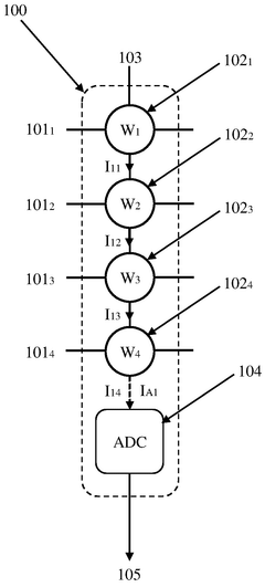
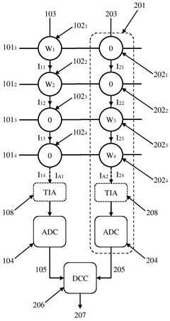
Innovation
- A crossbar structure with a plurality of input and output lines and cross-point devices, where at least one column has a zero weight to mitigate noise variations, and analog-to-digital converters with adjustable resolution to reduce power consumption, allowing for optimal trade-offs between reliability and complexity.
Scalable array architecture for in-memory computing
PatentPendingIN202227050313A
Innovation
- A scalable in-memory computing architecture with configurable Compute-In-Memory Units (CIMUs) interconnected via an on-chip network, employing charge-domain operation for high linearity and parallelism, and digital accumulation to overcome analog noise and enable integration in larger systems.
Energy Efficiency Considerations for In-Memory Computing Systems
Energy efficiency has emerged as a critical factor in the development and deployment of in-memory computing (IMC) systems based on crossbar arrays. As these architectures aim to overcome the von Neumann bottleneck by performing computations directly within memory, their power consumption characteristics become paramount for practical implementation at scale.
The fundamental energy consumption in crossbar-based IMC systems stems from three primary sources: read/write operations, computational processes, and peripheral circuitry overhead. During read operations, energy is consumed when sensing currents flow through memory cells, while write operations typically require higher voltage pulses that contribute significantly to overall power consumption. Computational energy is expended during matrix-vector multiplications and other operations performed within the crossbar structure.
Recent research has demonstrated several promising approaches to enhance energy efficiency. Dynamic voltage scaling techniques allow for adaptive adjustment of operating voltages based on computational requirements, potentially reducing energy consumption by 30-45% during less demanding operations. Precision-aware computing methods that match computational precision to application needs have shown energy savings of up to 60% with minimal accuracy loss in neural network applications.
Material innovations represent another frontier for energy optimization. Alternative resistive materials with lower switching energies, such as hafnium oxide and tantalum oxide compounds, have demonstrated switching energies below 1 pJ per transition. These materials enable significant power reductions while maintaining reliability metrics essential for commercial viability.
Circuit-level optimizations, including sense amplifier designs with reduced static power consumption and energy-efficient peripheral circuits, have contributed to lowering the energy footprint of crossbar systems. Advanced sensing schemes that minimize the voltage swing required for reliable operation have shown particular promise, reducing read energy by up to 40% compared to conventional approaches.
System-level energy management strategies, such as selective activation of crossbar regions and intelligent data mapping to minimize unnecessary operations, provide additional efficiency gains. These approaches become increasingly important as crossbar arrays scale to larger dimensions, where leakage currents and parasitic effects can dominate energy consumption profiles.
The energy efficiency landscape for crossbar-based IMC systems presents a complex optimization challenge that spans device physics, circuit design, and system architecture. Achieving the theoretical energy advantages of in-memory computing requires holistic approaches that address inefficiencies at each level of the design hierarchy.
Fabrication Techniques and Material Science Advancements
The evolution of fabrication techniques for crossbar arrays has been pivotal in advancing in-memory computing systems. Traditional CMOS fabrication processes initially provided the foundation, but specialized techniques have emerged to address the unique requirements of crossbar architectures. Atomic Layer Deposition (ALD) has become particularly significant, enabling precise control over thin film growth at the atomic scale, which is essential for creating uniform resistive switching layers in memristive devices.
Nanoimprint lithography represents another breakthrough, allowing for high-throughput patterning of nanoscale features with resolution beyond conventional photolithography limits. This technique has proven invaluable for creating dense crossbar arrays with minimal feature sizes, directly contributing to increased integration density and system scalability.
Material science advancements have paralleled these fabrication innovations. The transition from conventional metal-oxide materials to complex oxides like HfOx, TaOx, and TiOx has dramatically improved switching characteristics and reliability. These materials exhibit superior endurance, retention, and uniformity properties, addressing key challenges in resistive memory technologies.
Two-dimensional materials represent the frontier of crossbar array development. Graphene, MoS2, and other 2D materials offer atomically thin conducting layers with exceptional electrical properties. Their integration into crossbar structures enables unprecedented scaling potential while maintaining electrical performance. The inherent thinness of these materials also contributes to reduced parasitic capacitance, enhancing overall system speed.
Interface engineering has emerged as a critical focus area, with researchers developing specialized barrier layers and interface treatments to control ion migration and improve switching uniformity. These techniques have significantly enhanced device-to-device consistency, a prerequisite for large-scale arrays.
Advanced doping strategies for resistive switching materials have enabled fine-tuning of electrical characteristics. Controlled introduction of dopants modifies vacancy concentration and distribution, allowing engineers to optimize switching voltages, ON/OFF ratios, and retention characteristics according to specific application requirements.
Multi-layer stacking techniques have evolved to enable true 3D integration of crossbar arrays. Through precise alignment and interconnection methods, these approaches dramatically increase storage density and computational capability per unit area, representing a significant advancement toward highly scalable in-memory computing architectures.
Unlock deeper insights with Patsnap Eureka Quick Research — get a full tech report to explore trends and direct your research. Try now!
Generate Your Research Report Instantly with AI Agent
Supercharge your innovation with Patsnap Eureka AI Agent Platform!