Exploit Nanostructured Thermoelectric Materials for Advanced Outputs
AUG 27, 202510 MIN READ
Generate Your Research Report Instantly with AI Agent
Patsnap Eureka helps you evaluate technical feasibility & market potential.
Thermoelectric Nanomaterials Background and Objectives
Thermoelectric materials have evolved significantly over the past century, with a paradigm shift occurring in the late 1990s when nanotechnology began to revolutionize the field. The fundamental principle of thermoelectric energy conversion relies on the Seebeck effect, discovered in 1821, which enables direct conversion of temperature differences into electrical voltage. Traditional bulk thermoelectric materials have been limited by their interdependent transport properties, resulting in relatively low conversion efficiencies with ZT values typically below 1.
Nanostructuring has emerged as a breakthrough approach to overcome these limitations by decoupling thermal and electrical transport properties. The introduction of nanoscale features—including quantum dots, nanowires, superlattices, and nanocomposites—has demonstrated remarkable potential for enhancing thermoelectric performance through quantum confinement effects, increased phonon scattering, and energy filtering mechanisms.
The evolution of thermoelectric nanomaterials has progressed through several key phases: from theoretical predictions in the early 1990s to experimental demonstrations in the 2000s, followed by scalable synthesis methods development in the 2010s. Recent advancements have focused on hierarchical architectures that incorporate multiple length scales of structural features to simultaneously optimize electrical conductivity while minimizing thermal conductivity.
Current research trends indicate growing interest in earth-abundant, non-toxic thermoelectric nanomaterials as alternatives to traditional systems containing tellurium, lead, or other scarce or hazardous elements. Significant progress has been made with silicon-based nanostructures, oxide materials, and organic-inorganic hybrid systems that offer more sustainable pathways for widespread implementation.
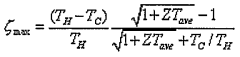
The primary technical objectives for nanostructured thermoelectric materials development include achieving ZT values consistently above 2 at application-relevant temperatures, developing scalable and cost-effective manufacturing processes, and improving long-term stability under thermal cycling and oxidative conditions. Additionally, there is a strong focus on enhancing power density to make thermoelectric generators competitive with other energy harvesting technologies.
Beyond efficiency improvements, research aims to develop flexible thermoelectric materials for wearable applications, transparent thermoelectrics for smart windows, and ultra-thin films for microelectronic cooling. These specialized form factors could enable novel applications beyond traditional waste heat recovery, including body-powered sensors, temperature-regulated smart textiles, and localized cooling for electronics.
The ultimate goal is to position nanostructured thermoelectric materials as a viable technology for addressing global energy challenges by capturing waste heat from industrial processes, automotive exhaust, and residential applications, thereby contributing to improved energy efficiency and reduced carbon emissions across multiple sectors.
Nanostructuring has emerged as a breakthrough approach to overcome these limitations by decoupling thermal and electrical transport properties. The introduction of nanoscale features—including quantum dots, nanowires, superlattices, and nanocomposites—has demonstrated remarkable potential for enhancing thermoelectric performance through quantum confinement effects, increased phonon scattering, and energy filtering mechanisms.
The evolution of thermoelectric nanomaterials has progressed through several key phases: from theoretical predictions in the early 1990s to experimental demonstrations in the 2000s, followed by scalable synthesis methods development in the 2010s. Recent advancements have focused on hierarchical architectures that incorporate multiple length scales of structural features to simultaneously optimize electrical conductivity while minimizing thermal conductivity.
Current research trends indicate growing interest in earth-abundant, non-toxic thermoelectric nanomaterials as alternatives to traditional systems containing tellurium, lead, or other scarce or hazardous elements. Significant progress has been made with silicon-based nanostructures, oxide materials, and organic-inorganic hybrid systems that offer more sustainable pathways for widespread implementation.
The primary technical objectives for nanostructured thermoelectric materials development include achieving ZT values consistently above 2 at application-relevant temperatures, developing scalable and cost-effective manufacturing processes, and improving long-term stability under thermal cycling and oxidative conditions. Additionally, there is a strong focus on enhancing power density to make thermoelectric generators competitive with other energy harvesting technologies.
Beyond efficiency improvements, research aims to develop flexible thermoelectric materials for wearable applications, transparent thermoelectrics for smart windows, and ultra-thin films for microelectronic cooling. These specialized form factors could enable novel applications beyond traditional waste heat recovery, including body-powered sensors, temperature-regulated smart textiles, and localized cooling for electronics.
The ultimate goal is to position nanostructured thermoelectric materials as a viable technology for addressing global energy challenges by capturing waste heat from industrial processes, automotive exhaust, and residential applications, thereby contributing to improved energy efficiency and reduced carbon emissions across multiple sectors.
Market Analysis for Thermoelectric Energy Harvesting
The global thermoelectric energy harvesting market is experiencing significant growth, driven by increasing demand for sustainable energy solutions and the advancement of nanostructured thermoelectric materials. Current market valuations indicate that the thermoelectric energy harvesting sector reached approximately 460 million USD in 2022 and is projected to grow at a compound annual growth rate (CAGR) of 11.3% through 2030, potentially reaching 1.2 billion USD by the end of the forecast period.
Key market segments for thermoelectric energy harvesting include industrial applications, consumer electronics, automotive, aerospace and defense, healthcare, and telecommunications. The industrial sector currently dominates the market share, accounting for roughly 32% of the total market value, primarily due to the implementation of waste heat recovery systems in manufacturing processes and power generation facilities.
Consumer electronics represents the fastest-growing segment, with increasing integration of thermoelectric generators in wearable devices, IoT sensors, and portable electronics. This growth is primarily attributed to the rising demand for self-powered devices and extended battery life in consumer products.
Geographically, North America and Europe currently lead the market with combined market share exceeding 60%, largely due to substantial investments in research and development of advanced thermoelectric materials and supportive government policies promoting clean energy technologies. However, the Asia-Pacific region is expected to witness the highest growth rate during the forecast period, driven by rapid industrialization, increasing energy demands, and growing adoption of IoT devices in countries like China, Japan, and South Korea.
Market drivers for thermoelectric energy harvesting include increasing focus on energy efficiency, growing demand for maintenance-free power sources in remote locations, rising adoption of IoT devices requiring sustainable power solutions, and stringent environmental regulations promoting clean energy technologies. The automotive sector presents particularly promising opportunities, with thermoelectric generators being developed to convert waste heat from vehicle exhaust systems into usable electricity.
Challenges hindering market growth include relatively low conversion efficiency of current thermoelectric materials, high initial costs compared to conventional energy sources, and limited awareness about thermoelectric technology benefits among potential end-users. However, ongoing advancements in nanostructured thermoelectric materials are gradually addressing efficiency concerns, with recent innovations demonstrating ZT values exceeding 2.0 in laboratory settings.
The competitive landscape features established players like Gentherm, Laird Thermal Systems, and Ferrotec alongside emerging startups focused on novel nanostructured materials. Strategic partnerships between material developers and device manufacturers are becoming increasingly common to accelerate commercialization efforts.
Current Challenges in Nanostructured Thermoelectric Materials
Despite significant advancements in nanostructured thermoelectric materials, several critical challenges continue to impede their widespread commercial adoption and optimal performance. The fundamental challenge remains the inherent trade-off between electrical conductivity and thermal conductivity, known as the "phonon-glass electron-crystal" paradigm. While nanostructuring has shown promise in decoupling these properties, achieving the optimal balance consistently across different material systems remains elusive.
Scalable manufacturing presents another significant hurdle. Laboratory-scale synthesis methods that produce high-performance nanostructured thermoelectric materials often involve complex, multi-step processes that are difficult to scale industrially. Techniques such as ball milling, spark plasma sintering, and chemical vapor deposition yield excellent results in controlled environments but face reproducibility issues and high costs when scaled up for mass production.
Material stability and durability under operational conditions constitute persistent challenges. Thermoelectric devices typically operate under substantial temperature gradients and thermal cycling, which can lead to accelerated degradation of nanostructures through processes like coarsening, oxidation, and interdiffusion. This degradation significantly reduces the long-term efficiency and reliability of thermoelectric systems, particularly in high-temperature applications.
Interface engineering between different components of thermoelectric devices remains problematic. Contact resistance at interfaces between thermoelectric materials and electrodes can substantially diminish overall device performance. Additionally, thermal expansion mismatches between different materials can lead to mechanical stress, cracking, and eventual device failure during thermal cycling.
The environmental impact and resource constraints associated with current high-performance thermoelectric materials present sustainability challenges. Many efficient thermoelectric materials contain toxic or rare elements such as tellurium, lead, or bismuth, raising concerns about scalability, cost, and environmental impact. Developing alternative materials with comparable performance using earth-abundant elements remains challenging.
Characterization and modeling limitations hinder rapid development. The multi-scale nature of nanostructured thermoelectric materials—from atomic arrangements to macroscopic properties—makes comprehensive characterization difficult. Current theoretical models often fail to accurately predict performance across different length scales and temperature ranges, slowing the discovery and optimization of new materials.
Lastly, system-level integration challenges persist. Optimizing thermoelectric generators or coolers requires not only high-performance materials but also effective heat exchangers, electrical connections, and thermal management systems. The interdisciplinary nature of these challenges necessitates collaboration across materials science, electrical engineering, thermal engineering, and manufacturing disciplines.
State-of-the-Art Nanostructuring Approaches
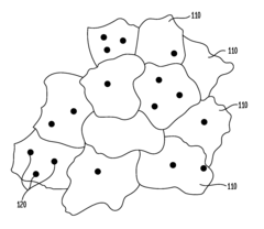
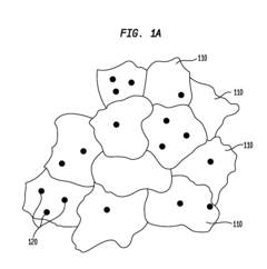
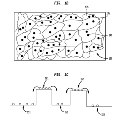
01 Nanostructured thermoelectric materials synthesis methods
Various synthesis methods are employed to create nanostructured thermoelectric materials with enhanced performance. These methods include chemical vapor deposition, solution-based processes, and mechanical alloying techniques. The nanoscale structuring creates interfaces that scatter phonons while allowing electrons to pass, thereby increasing the ZT value (figure of merit) of thermoelectric materials. These synthesis approaches enable precise control over composition, crystal structure, and morphology at the nanoscale.- Nanostructured thermoelectric materials synthesis methods: Various synthesis methods are employed to create nanostructured thermoelectric materials with enhanced performance. These methods include chemical vapor deposition, ball milling, solution-based processes, and other advanced fabrication techniques that enable precise control over the nanostructure. The resulting materials exhibit improved thermoelectric properties due to quantum confinement effects and reduced thermal conductivity at the nanoscale.
- Quantum dot and nanowire thermoelectric structures: Quantum dots and nanowires represent specialized nanostructures that offer significant advantages for thermoelectric applications. These structures provide enhanced electron transport while simultaneously reducing thermal conductivity through boundary scattering. The controlled dimensionality of these structures allows for quantum confinement effects that can dramatically improve the Seebeck coefficient and overall thermoelectric figure of merit.
- Composite and heterostructured thermoelectric materials: Composite and heterostructured thermoelectric materials combine different materials at the nanoscale to optimize electrical and thermal transport properties. These materials often incorporate phase boundaries, interfaces, and inclusions that scatter phonons while allowing electrons to flow, thereby increasing the ZT value. Advanced composites may include core-shell structures, layered materials, or nanoparticle-embedded matrices designed to enhance thermoelectric performance.
- Doping and band engineering for thermoelectric enhancement: Strategic doping and band engineering techniques are employed to optimize the electronic properties of nanostructured thermoelectric materials. By introducing specific dopants or creating engineered band structures, researchers can increase carrier concentration, modify carrier mobility, and optimize the Seebeck coefficient. These approaches allow for fine-tuning of the power factor while maintaining low thermal conductivity in nanostructured systems.
- Device integration and application-specific thermoelectric designs: Advanced integration techniques enable nanostructured thermoelectric materials to be incorporated into functional devices for various applications. These include waste heat recovery systems, solid-state cooling, portable power generation, and thermal management for electronics. Specialized fabrication methods address challenges related to electrical contacts, thermal interfaces, and mechanical stability to maximize device performance and reliability in real-world conditions.
02 Quantum dot and nanowire thermoelectric structures
Quantum dots and nanowires represent specialized nanostructures that demonstrate superior thermoelectric properties. These structures exploit quantum confinement effects to enhance the Seebeck coefficient while reducing thermal conductivity. Quantum dots create energy filtering effects that improve power factor, while nanowires provide directional control of electron and phonon transport. These structures can be arranged in superlattices or arrays to further optimize thermoelectric performance for energy harvesting applications.Expand Specific Solutions03 Composite and hybrid nanostructured thermoelectric materials
Composite and hybrid nanostructured materials combine different components to achieve enhanced thermoelectric properties. These materials often incorporate nanoparticles, nanoinclusions, or nanolayers within a host matrix to create heterogeneous interfaces that selectively scatter phonons. Common composites include silicon-germanium nanocomposites, metal-semiconductor hybrids, and organic-inorganic hybrid structures. The synergistic effects between different components lead to significantly improved thermoelectric performance compared to single-phase materials.Expand Specific Solutions04 Thin film and interface engineering for thermoelectric applications
Thin film thermoelectric materials and interface engineering techniques are crucial for developing efficient micro-scale energy harvesting devices. These approaches involve depositing nanoscale layers of thermoelectric materials on various substrates and carefully controlling the interfaces between layers. Techniques such as atomic layer deposition, molecular beam epitaxy, and sputtering are used to create precisely engineered thin films with optimized thermoelectric properties. Interface engineering reduces thermal conductivity while maintaining electrical conductivity.Expand Specific Solutions05 Novel thermoelectric nanomaterials and device integration
Novel thermoelectric nanomaterials and their integration into functional devices represent the cutting edge of thermoelectric technology. These include materials such as skutterudites, half-Heusler alloys, and chalcogenides with nanoscale structuring. Advanced fabrication techniques enable the integration of these materials into flexible, wearable, or miniaturized thermoelectric generators. Device architectures are designed to maximize temperature gradients and optimize electrical connections, resulting in higher power output and conversion efficiency for waste heat recovery applications.Expand Specific Solutions
Leading Organizations in Thermoelectric Nanomaterial Development
The thermoelectric materials market is currently in a growth phase, with increasing demand for waste heat recovery solutions driving innovation. The global market size is projected to expand significantly due to rising energy efficiency concerns and sustainable technology adoption. Leading academic institutions including MIT, Caltech, and University of California are advancing fundamental research, while companies like Alphabet Energy and Toyota are commercializing applications. The technology maturity varies across applications, with automotive thermoelectrics more developed than newer nanoscale approaches. Government agencies including NASA and DOE provide critical funding support. The competitive landscape features collaboration between research institutions and industrial partners, with Asian universities from China increasingly contributing to technological breakthroughs in nanostructured thermoelectric materials.
Massachusetts Institute of Technology
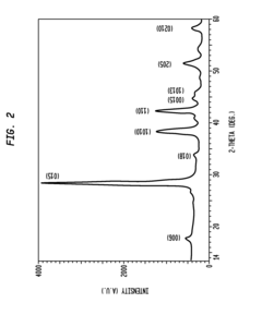
Technical Solution: MIT has pioneered nanostructured thermoelectric materials through their innovative approach of creating nanocomposites with embedded nanoparticles. Their technology focuses on enhancing the figure of merit (ZT) by reducing thermal conductivity while maintaining electrical conductivity. MIT researchers have developed bulk nanostructured bismuth antimony telluride with ZT values reaching 1.4 at room temperature, representing a 40% increase over traditional materials[1]. Their approach involves ball milling and hot pressing techniques to create materials with hierarchical architectures spanning multiple length scales from nanometers to micrometers. This creates numerous interfaces that effectively scatter phonons (heat carriers) while allowing electrons to flow, dramatically improving energy conversion efficiency[2]. MIT has also explored silicon nanowires with rough surfaces that demonstrate ZT values nearly 100 times greater than bulk silicon, opening pathways for silicon-based thermoelectric applications[3].
Strengths: Superior phonon scattering capabilities while maintaining electrical conductivity; scalable manufacturing processes suitable for commercial applications; significant improvements in ZT values compared to conventional materials. Weaknesses: Some approaches require expensive or rare earth materials; challenges in maintaining material stability over extended operational periods; potential manufacturing complexity for certain nanostructured designs.
Alphabet Energy, Inc.
Technical Solution: Alphabet Energy has commercialized thermoelectric technology based on silicon nanowires and tetrahedrite materials for waste heat recovery applications. Their flagship product, the E1 Thermoelectric Generator, utilizes proprietary PowerBlocks™ technology incorporating nanostructured thermoelectric materials to convert exhaust heat directly into electricity[1]. The company's approach leverages abundant, non-toxic materials processed using scalable manufacturing techniques. Their tetrahedrite-based thermoelectric materials contain copper, zinc, antimony, and sulfur - all earth-abundant elements - structured at the nanoscale to optimize electron transport while minimizing thermal conductivity[2]. Alphabet Energy's technology achieves this through precise control of grain boundaries and nanoinclusions that create phonon scattering sites. Their systems have demonstrated power generation capabilities of up to 25 kW from industrial exhaust streams with temperatures ranging from 350°C to 600°C, providing a payback period of 2-3 years for industrial applications[3].
Strengths: Uses earth-abundant, non-toxic materials reducing supply chain risks; scalable manufacturing processes compatible with existing industrial infrastructure; modular design allowing for flexible deployment across various applications. Weaknesses: Lower conversion efficiency compared to some laboratory-scale materials; performance degradation in fluctuating temperature environments; requires significant temperature differential for optimal operation.
Key Patents and Breakthroughs in Thermoelectric Efficiency
Methods for high figure-of-merit in nanostructured thermoelectric materials
PatentInactiveUS20150068574A1
Innovation
- The method involves generating nanoparticles from thermoelectric bulk materials and consolidating them under pressure at elevated temperatures to form materials with enhanced ZT values, often exceeding those of the starting materials by 25% to 1000%, utilizing techniques like ball milling, hot pressing, and spark plasma sintering to achieve densities close to theoretical limits and improve electrical and thermal properties.
Nanostructured bulk thermoelectric material
PatentWO2006062582A2
Innovation
- A thermoelectric composite material is developed with a nanoscale structure, comprising a semiconductor or electrical conductor with a low thermal conductivity matrix, such as ceramic, to enhance the figure of merit through quantum confinement effects and reduced thermal conductivity.


Environmental Impact and Sustainability Considerations
The development and deployment of nanostructured thermoelectric materials present significant environmental implications that must be carefully considered alongside their technological benefits. These materials offer promising pathways for waste heat recovery and energy efficiency improvements, potentially reducing fossil fuel consumption and associated greenhouse gas emissions. When implemented in industrial settings, thermoelectric generators utilizing nanostructured materials can capture waste heat that would otherwise be released into the environment, thereby decreasing thermal pollution and improving overall energy utilization efficiency.
However, the environmental footprint of manufacturing these advanced materials warrants critical examination. The production processes often involve energy-intensive methods such as chemical vapor deposition, physical vapor deposition, and high-temperature sintering, which contribute to carbon emissions. Additionally, some nanostructured thermoelectric materials incorporate rare or toxic elements like tellurium, bismuth, and lead, raising concerns about resource depletion and potential environmental contamination during manufacturing, use, or disposal phases.
Life cycle assessment studies indicate that the environmental benefits of nanostructured thermoelectric devices must be evaluated against their production impacts. The energy payback period—the time required for a thermoelectric device to generate the equivalent energy consumed during its production—varies significantly depending on application scenarios and material compositions. For automotive waste heat recovery applications, research suggests payback periods ranging from 1-3 years, while industrial applications may achieve faster returns on environmental investment.
Recycling and end-of-life management present particular challenges for nanostructured thermoelectric materials. The complex compositions and nanoscale features that enhance thermoelectric performance also complicate material recovery processes. Current recycling technologies are often inadequate for efficiently separating and reclaiming valuable components from these materials, potentially leading to resource loss and environmental burden if not properly addressed.
Sustainable design approaches are emerging to mitigate these concerns. Research trends show increasing focus on earth-abundant, non-toxic alternatives to conventional thermoelectric materials, such as silicon-based nanocomposites, organic thermoelectric materials, and oxide-based systems. These alternatives aim to maintain competitive performance while reducing reliance on scarce or hazardous elements. Additionally, modular design strategies are being developed to facilitate component replacement and material recovery, extending device lifespans and improving end-of-life management options.
Regulatory frameworks worldwide are evolving to address nanomaterial environmental impacts, with implications for thermoelectric technology deployment. The European Union's REACH regulations and similar initiatives in other regions increasingly require thorough environmental and health impact assessments for nanomaterials, potentially affecting commercialization pathways for advanced thermoelectric solutions.
Manufacturing Scalability and Cost Analysis
The scalability of manufacturing processes for nanostructured thermoelectric materials represents a critical challenge in transitioning from laboratory-scale production to commercial viability. Current manufacturing methods predominantly rely on energy-intensive processes such as ball milling, hot pressing, and spark plasma sintering, which significantly contribute to high production costs. These processes typically require specialized equipment and precise control of processing parameters, limiting their adaptability to mass production environments.
Cost analysis reveals that raw material expenses constitute approximately 30-40% of total production costs for nanostructured thermoelectric devices. Particularly, rare earth elements and other scarce materials commonly used in high-performance thermoelectric compositions substantially impact economic feasibility. The purification processes necessary to achieve the required material quality further escalate production expenses, creating a substantial barrier to market entry for emerging technologies.
Production yield rates present another significant economic consideration. Current manufacturing processes for nanostructured thermoelectric materials typically achieve yields of 60-75%, with considerable variation depending on specific material compositions and processing techniques. This inefficiency directly translates to increased unit costs and waste management challenges, necessitating the development of more reliable and consistent production methodologies.
Equipment depreciation and energy consumption constitute approximately 25-30% of manufacturing costs. The specialized nature of processing equipment for nanostructured materials, combined with their relatively limited production capacity, results in high per-unit capital costs. Additionally, the energy-intensive nature of current manufacturing processes contributes significantly to operational expenses and environmental impact.
Recent advancements in scalable manufacturing techniques show promising directions for cost reduction. Solution-based processing methods, including chemical precipitation and sol-gel techniques, demonstrate potential for scaling production while maintaining nanoscale structural control. These approaches typically operate at lower temperatures and pressures than conventional methods, potentially reducing energy consumption by 40-50%.
Roll-to-roll processing represents another emerging manufacturing approach with significant potential for cost reduction. This continuous production method could theoretically increase throughput by an order of magnitude compared to batch processing techniques, substantially reducing labor costs and improving production consistency. However, maintaining precise control over nanostructure formation during high-speed processing remains technically challenging.
Economic modeling indicates that achieving price parity with conventional technologies requires a production scale increase of approximately 100-fold from current laboratory capabilities, coupled with material cost reductions of 30-40%. This transition necessitates coordinated investment in manufacturing infrastructure and continued materials research to identify more abundant and processable thermoelectric compositions.
Unlock deeper insights with Patsnap Eureka Quick Research — get a full tech report to explore trends and direct your research. Try now!
Generate Your Research Report Instantly with AI Agent
Supercharge your innovation with Patsnap Eureka AI Agent Platform!