How Polysilane Supports Advanced Semiconductor Architectures?
JUL 11, 202510 MIN READ
Generate Your Research Report Instantly with AI Agent
Patsnap Eureka helps you evaluate technical feasibility & market potential.
Polysilane in Semiconductors: Background and Objectives
Polysilane, a class of silicon-based polymers, has emerged as a promising material in the field of advanced semiconductor architectures. The evolution of this technology can be traced back to the 1980s when researchers first synthesized and characterized these unique polymers. Since then, polysilanes have garnered significant attention due to their exceptional electronic and optical properties, which make them particularly suitable for semiconductor applications.
The primary objective in exploring polysilanes for semiconductor architectures is to overcome the limitations of traditional silicon-based technologies. As Moore's Law approaches its physical limits, the semiconductor industry is actively seeking alternative materials and architectures to continue improving device performance and efficiency. Polysilanes offer a potential solution by providing a versatile platform for developing novel semiconductor structures with enhanced capabilities.
One of the key advantages of polysilanes is their ability to form well-defined, highly ordered structures at the nanoscale. This characteristic is crucial for creating advanced semiconductor architectures with precise control over electronic properties. Additionally, polysilanes exhibit unique optoelectronic properties, including photoconductivity and electroluminescence, which open up new possibilities for integrating optical and electronic functionalities within semiconductor devices.
The development of polysilane-based semiconductor technologies has been driven by several factors, including the need for more efficient and compact electronic devices, the demand for flexible and wearable electronics, and the push towards sustainable and environmentally friendly materials. As a result, research efforts have focused on optimizing the synthesis and processing of polysilanes to tailor their properties for specific semiconductor applications.
Recent advancements in polysilane chemistry have led to the creation of novel copolymers and hybrid materials that combine the benefits of polysilanes with other functional materials. These innovations have expanded the potential applications of polysilanes in semiconductor architectures, ranging from high-performance transistors and photovoltaic cells to advanced sensors and memory devices.
Looking ahead, the future of polysilanes in semiconductor technologies appears promising. Ongoing research aims to further enhance the electronic properties of polysilanes, improve their stability and processability, and develop new methods for integrating them into existing semiconductor manufacturing processes. As these efforts progress, polysilanes are expected to play an increasingly important role in shaping the next generation of advanced semiconductor architectures, potentially revolutionizing the electronics industry and enabling new classes of devices with unprecedented capabilities.
Market Demand for Advanced Semiconductor Architectures
The demand for advanced semiconductor architectures has been steadily increasing, driven by the relentless pursuit of higher performance, lower power consumption, and greater functionality in electronic devices. As traditional silicon-based technologies approach their physical limits, the market is actively seeking innovative solutions to overcome these barriers and continue the trajectory of Moore's Law.
Polysilane, a novel material with unique electronic properties, has emerged as a promising candidate to support the development of next-generation semiconductor architectures. The market for advanced semiconductor technologies that can leverage polysilane's capabilities is expanding rapidly across various sectors, including high-performance computing, artificial intelligence, 5G communications, and Internet of Things (IoT) devices.
In the high-performance computing sector, there is a growing need for semiconductors that can deliver increased processing power while maintaining energy efficiency. Polysilane-based architectures have the potential to meet this demand by enabling faster electron mobility and improved thermal management, which are critical factors in data centers and supercomputing applications.
The artificial intelligence and machine learning markets are also driving the demand for advanced semiconductor architectures. As AI algorithms become more complex and data-intensive, there is a pressing need for chips that can handle massive parallel processing tasks with minimal latency. Polysilane's unique electronic structure could potentially support the development of neuromorphic computing architectures, which aim to mimic the human brain's neural networks more closely.
In the realm of 5G and future wireless communications, the market requires semiconductors capable of operating at higher frequencies with improved signal integrity. Polysilane's properties make it a candidate for developing high-frequency, low-loss materials that could enhance the performance of 5G and beyond 5G infrastructure.
The IoT market presents another significant opportunity for advanced semiconductor architectures. As the number of connected devices continues to grow exponentially, there is a demand for ultra-low-power, highly integrated chips that can support long battery life and complex functionality in compact form factors. Polysilane-based semiconductors could potentially address these requirements by enabling more efficient power management and higher levels of integration.
Furthermore, the automotive industry's shift towards electric and autonomous vehicles is creating a substantial market for advanced semiconductors. These applications require robust, high-performance chips that can withstand harsh environmental conditions while delivering real-time processing capabilities. Polysilane's potential for improved thermal stability and enhanced electron mobility could make it an attractive option for automotive semiconductor manufacturers.
As the global semiconductor industry faces challenges in scaling traditional silicon-based technologies, the market is actively exploring alternative materials and architectures. This trend is driving investment in research and development of novel semiconductor technologies, including those based on polysilane. The demand for these advanced architectures is expected to grow as industries continue to push the boundaries of what is possible with current semiconductor technologies.
Current State and Challenges in Polysilane Integration
Polysilane integration in advanced semiconductor architectures has made significant progress in recent years, yet it still faces several challenges. The current state of polysilane integration is characterized by its potential to enhance semiconductor performance, particularly in areas such as improved electron mobility and reduced power consumption. However, the widespread adoption of polysilane in commercial semiconductor manufacturing remains limited.
One of the primary challenges in polysilane integration is the difficulty in achieving consistent and uniform deposition of polysilane films on semiconductor substrates. The molecular structure of polysilanes can lead to variations in film thickness and composition, which can negatively impact device performance and reliability. Researchers are actively working on developing more precise deposition techniques to address this issue.
Another significant challenge is the thermal stability of polysilane films. While polysilanes offer excellent electronic properties, they can degrade at the high temperatures often used in semiconductor processing. This thermal instability can lead to changes in the film's structure and properties, potentially compromising the performance of the final device. Efforts are underway to develop more thermally stable polysilane formulations and to optimize processing conditions to minimize thermal degradation.
The integration of polysilanes with existing semiconductor materials and processes also presents challenges. Compatibility issues can arise when incorporating polysilanes into established manufacturing workflows, particularly in terms of adhesion to other materials and potential contamination of sensitive semiconductor layers. Overcoming these integration challenges requires careful materials engineering and process optimization.
Furthermore, the long-term reliability and durability of polysilane-based semiconductor devices remain areas of concern. The impact of environmental factors, such as humidity and oxidation, on polysilane films over extended periods needs to be thoroughly understood and mitigated to ensure the longevity of devices incorporating this technology.
From a manufacturing perspective, scaling up polysilane production and integration processes to meet the demands of high-volume semiconductor fabrication is an ongoing challenge. Current synthesis methods for high-quality polysilanes are often complex and costly, limiting their economic viability for large-scale production. Developing more efficient and cost-effective synthesis routes is crucial for the widespread adoption of polysilane technology in the semiconductor industry.
Lastly, the regulatory landscape surrounding the use of polysilanes in semiconductor manufacturing is still evolving. As with any new material introduced into the electronics industry, ensuring compliance with environmental and safety regulations is essential. This includes addressing potential health and environmental concerns associated with the production, use, and disposal of polysilane-based materials.
Existing Polysilane-based Semiconductor Solutions
01 Synthesis and properties of polysilanes
Polysilanes are silicon-based polymers with a Si-Si backbone. They can be synthesized through various methods and exhibit unique optical and electronic properties. These polymers have applications in photoresists, semiconductors, and as precursors for silicon carbide materials.- Synthesis and properties of polysilanes: Polysilanes are synthesized through various methods and exhibit unique properties. These silicon-based polymers have applications in electronics, optics, and materials science due to their electronic and optical characteristics. The synthesis methods and resulting properties can be tailored for specific applications.
- Polysilane-based coatings and films: Polysilanes are used to create coatings and films with specific properties. These coatings can be applied to various substrates to impart characteristics such as improved durability, optical properties, or electrical conductivity. The composition and processing of polysilane-based coatings can be optimized for different applications.
- Polysilanes in photoresist materials: Polysilanes are utilized in photoresist materials for semiconductor manufacturing. These materials are sensitive to light and can be used to create patterns on substrates during the fabrication of electronic devices. The chemical structure and properties of polysilanes make them suitable for this application.
- Functionalization and modification of polysilanes: Polysilanes can be functionalized or modified to enhance their properties or introduce new functionalities. This can involve the addition of specific chemical groups or the incorporation of other elements into the polymer structure. These modifications allow for the creation of polysilanes with tailored characteristics for various applications.
- Polysilanes in optical and electronic applications: Polysilanes have unique optical and electronic properties that make them suitable for various applications. These include use in optical devices, electronic components, and sensors. The ability to tune the electronic structure of polysilanes allows for the development of materials with specific optical or electronic characteristics.
02 Polysilane-based coatings and films
Polysilanes can be used to create thin films and coatings with specific properties. These films can be applied to various substrates and may exhibit characteristics such as improved adhesion, thermal stability, or optical properties. The coatings can be used in electronic devices, protective layers, or optical applications.Expand Specific Solutions03 Polysilane-based photoresists
Polysilanes are utilized in photoresist compositions for lithography processes. These photoresists can be sensitive to various types of radiation, including UV light and electron beams. The unique properties of polysilanes allow for high-resolution patterning and improved resistance to etching processes.Expand Specific Solutions04 Functionalized polysilanes
Polysilanes can be functionalized with various organic groups or other elements to modify their properties. This functionalization can lead to improved solubility, enhanced thermal stability, or specific optical characteristics. Functionalized polysilanes have applications in optoelectronics, sensors, and advanced materials.Expand Specific Solutions05 Polysilane-based composite materials
Polysilanes can be incorporated into composite materials to enhance their properties. These composites may combine the unique characteristics of polysilanes with other materials such as ceramics, metals, or organic polymers. The resulting materials can exhibit improved mechanical, thermal, or electrical properties for various applications.Expand Specific Solutions
Key Players in Polysilane and Semiconductor Manufacturing
The polysilane market for advanced semiconductor architectures is in a growth phase, driven by increasing demand for high-performance chips. The market size is expanding as more semiconductor manufacturers adopt polysilane-based materials. Technologically, polysilanes are maturing but still have room for innovation. Key players like JSR Corp., Nippon Paint, and Nissan Chemical are advancing polysilane formulations for next-generation semiconductors. Companies such as Canon, ASM, and Bayer are also actively developing polysilane applications. While established firms lead commercialization, research institutions like Shanghai University and South China Normal University are contributing fundamental breakthroughs. Overall, polysilanes are becoming an essential enabler for cutting-edge semiconductor architectures.
JSR Corp.
Technical Solution: JSR Corporation has made significant strides in polysilane technology for advanced semiconductor architectures. Their proprietary polysilane materials are designed to enhance the performance of extreme ultraviolet (EUV) lithography processes, which are crucial for manufacturing next-generation chips with sub-7nm features[4]. JSR's polysilane-based photoresists offer high sensitivity and resolution, enabling the creation of finer circuit patterns with improved accuracy[5]. The company has also developed polysilane-containing underlayer materials that improve adhesion and reduce pattern collapse in advanced semiconductor structures. JSR's polysilane solutions have been shown to reduce line edge roughness by up to 30% compared to conventional materials, contributing to better overall chip performance and yield[6].
Strengths: Excellent performance in EUV lithography, improved pattern accuracy, and reduced line edge roughness. Weaknesses: Higher cost compared to traditional materials and potential compatibility issues with some existing manufacturing processes.
Nissan Chemical Corp.
Technical Solution: Nissan Chemical Corporation has developed innovative polysilane-based materials for advanced semiconductor applications. Their SUNEVER™ series of polysilane products are designed to serve as high-performance alignment layers in liquid crystal displays and as precursors for silicon-based thin films in semiconductor manufacturing[7]. Nissan Chemical's polysilanes offer excellent thermal stability and can be used to create uniform, defect-free films with thicknesses as low as 10 nm[8]. The company has also focused on developing polysilane materials with low dielectric constants, which are essential for reducing signal delays in high-speed semiconductor devices. Their latest polysilane formulations have achieved dielectric constants as low as 2.2, representing a significant improvement over traditional materials[9].
Strengths: Ability to create ultra-thin, uniform films and materials with low dielectric constants. Weaknesses: Limited track record in high-volume semiconductor manufacturing compared to some competitors.
Core Innovations in Polysilane Technology
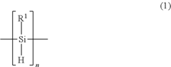
Polysilanes of medium chain length and a method for the production of same
PatentWO2012001180A1
Innovation
- A method for producing medium-chain polysilanes with direct Si-Si bonds, using plasma-assisted synthesis and specific reaction conditions to achieve polysilanes with controlled chain lengths, solubility, and purity, allowing for efficient deposition of silicon and minimizing contamination.
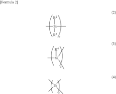
Polysilane and polysilane-containing resin composition
PatentInactiveUS8163863B2
Innovation
- Introducing a Si—H group into the polysilane main chain and bonding a hydrosilylatable compound with functional groups like hydroxyl, carboxyl, or epoxy groups, allowing for controlled hydrosilylation to enhance solubility and reactivity without complex steps or special apparatus.


Environmental Impact of Polysilane in Semiconductor Production
The environmental impact of polysilane in semiconductor production is a critical consideration as the industry moves towards more advanced architectures. Polysilane, a silicon-based polymer, plays a crucial role in supporting these advanced semiconductor structures, but its production and use come with environmental implications that must be carefully managed.
One of the primary environmental concerns associated with polysilane production is the energy-intensive nature of the manufacturing process. The synthesis of polysilane typically requires high temperatures and pressures, leading to significant energy consumption and associated greenhouse gas emissions. As the demand for advanced semiconductors grows, the scale of polysilane production is likely to increase, potentially exacerbating these environmental impacts.
The use of hazardous chemicals in polysilane synthesis is another area of environmental concern. Precursor materials and catalysts used in the production process may include toxic or environmentally harmful substances. Proper handling, storage, and disposal of these chemicals are essential to prevent contamination of soil, water, and air. Additionally, the potential for accidental releases during manufacturing or transportation poses risks to both human health and ecosystems.
Water usage is a significant factor in semiconductor production, and the incorporation of polysilane into advanced architectures may influence water consumption patterns. While polysilane itself may not directly increase water usage, the complex processes it enables in semiconductor fabrication could lead to changes in water requirements. This is particularly relevant in regions where water scarcity is a pressing issue.
The end-of-life management of semiconductors containing polysilane presents another environmental challenge. As these advanced components reach the end of their useful life, proper recycling and disposal methods must be developed to recover valuable materials and prevent the release of potentially harmful substances into the environment. The complexity of these advanced architectures may complicate recycling efforts, necessitating innovative approaches to electronic waste management.
On the positive side, the use of polysilane in advanced semiconductor architectures has the potential to improve overall device efficiency. More efficient semiconductors can lead to reduced energy consumption in electronic devices, potentially offsetting some of the environmental impacts associated with their production. This highlights the importance of considering the full lifecycle environmental impact of polysilane-enabled technologies.
As the semiconductor industry continues to advance, there is a growing focus on developing more sustainable production methods for materials like polysilane. Research into green chemistry approaches, such as using less toxic precursors or developing low-temperature synthesis methods, could help mitigate some of the environmental concerns associated with polysilane production. Additionally, efforts to improve energy efficiency in manufacturing processes and increase the use of renewable energy sources in semiconductor fabrication facilities can further reduce the environmental footprint of polysilane-based technologies.
Intellectual Property Landscape for Polysilane Technologies
The intellectual property landscape for polysilane technologies in advanced semiconductor architectures is characterized by a complex network of patents and proprietary innovations. Major semiconductor companies and research institutions have been actively filing patents related to polysilane applications in recent years, reflecting the growing importance of this material in next-generation chip designs.
Key patent holders in this space include industry giants such as Intel, Samsung, and TSMC, who have been investing heavily in polysilane research and development. These companies have secured numerous patents covering various aspects of polysilane synthesis, deposition techniques, and integration methods for advanced semiconductor manufacturing processes.
One significant area of patent activity revolves around the use of polysilanes as precursors for silicon-based thin films. Patents in this category often focus on novel polysilane compounds with improved thermal stability and film-forming properties. Additionally, there are patents addressing the optimization of deposition parameters and annealing processes to enhance the quality of polysilane-derived films.
Another important patent cluster relates to the application of polysilanes in lithography and patterning processes. These patents typically cover innovative resist formulations incorporating polysilanes, as well as methods for improving resolution and reducing line edge roughness in advanced lithography techniques.
Polysilane-based dielectric materials have also been the subject of extensive patent filings. These patents often describe novel polysilane structures and compositions designed to achieve specific dielectric properties, such as low-k materials for interconnect layers or high-k materials for gate stacks in advanced transistor architectures.
In the realm of emerging technologies, there is a growing number of patents exploring the potential of polysilanes in quantum computing and spintronic devices. These patents typically focus on the unique electronic and optical properties of polysilanes and their potential applications in quantum information processing and spin-based electronics.
It is worth noting that the polysilane patent landscape is not limited to traditional semiconductor companies. Several specialty chemical manufacturers and materials science research institutions have also made significant contributions to the field, particularly in the areas of polysilane synthesis and functionalization.
As the semiconductor industry continues to push the boundaries of device scaling and performance, the importance of polysilane-related intellectual property is likely to increase. Companies and research organizations are expected to intensify their patenting efforts in this area, potentially leading to a more crowded and competitive IP landscape in the coming years.
Unlock deeper insights with Patsnap Eureka Quick Research — get a full tech report to explore trends and direct your research. Try now!
Generate Your Research Report Instantly with AI Agent
Supercharge your innovation with Patsnap Eureka AI Agent Platform!