Research on Volumetric 3D printing for high performance electronics and micro devices
SEP 28, 202510 MIN READ
Generate Your Research Report Instantly with AI Agent
Patsnap Eureka helps you evaluate technical feasibility & market potential.
Volumetric 3D Printing Evolution and Objectives
Volumetric 3D printing represents a paradigm shift in additive manufacturing technology, evolving from traditional layer-by-layer approaches to a revolutionary process that simultaneously solidifies an entire volume of material. This technique emerged in the early 2010s as researchers sought to overcome the speed limitations and mechanical anisotropy inherent in conventional 3D printing methods. The evolution began with computed axial lithography (CAL), which uses synchronized projections of light patterns into photosensitive resins to create complex structures in seconds rather than hours.
The technology has progressed through several key developmental phases, starting with proof-of-concept demonstrations in academic laboratories, followed by refinement of optical systems and photochemistry to enhance resolution and material compatibility. Recent advancements have focused on expanding the range of printable materials to include functional polymers, ceramics, and even biological tissues, significantly broadening potential applications in electronics and microdevices.
A critical milestone in volumetric 3D printing evolution was the integration of digital light processing (DLP) technology with sophisticated algorithms for tomographic reconstruction, enabling precise control over the solidification process throughout the entire volume. This integration has dramatically improved both printing speed and resolution, with some systems now capable of sub-micron precision across centimeter-scale objects.
The primary objective of volumetric 3D printing research for high-performance electronics and microdevices is to develop manufacturing processes that can produce complex, multi-material structures with embedded functionality at scales relevant to modern electronics. This includes creating conductive pathways, semiconductor components, and sensing elements within a single printing process, eliminating the need for multiple fabrication steps and assembly operations.
Additional technical goals include enhancing the electrical and thermal properties of printed materials to match or exceed those of conventionally manufactured components, improving the resolution to accommodate the increasingly miniaturized nature of electronic devices, and developing compatible materials that can withstand the operational demands of high-performance electronics.
The technology aims to enable rapid prototyping and customization of electronic components, potentially revolutionizing product development cycles and enabling new design paradigms that are currently constrained by traditional manufacturing limitations. Researchers are particularly focused on achieving multi-material printing capabilities that can seamlessly integrate conductors, semiconductors, and insulators within a single volumetric printing process.
Long-term objectives include developing systems capable of printing fully functional electronic devices with integrated circuits, sensors, and actuators in a single operation, potentially transforming electronics manufacturing from a complex, multi-step process to a streamlined, digitally driven production method suitable for both mass production and customized, small-batch manufacturing scenarios.
Market Analysis for Advanced Electronics Manufacturing
The global market for advanced electronics manufacturing is experiencing unprecedented growth, driven by the emergence of volumetric 3D printing technologies. This revolutionary approach to fabrication is reshaping traditional manufacturing paradigms, particularly in high-performance electronics and microdevices sectors. Current market valuations indicate that the advanced electronics manufacturing industry is projected to reach $2.1 trillion by 2025, with volumetric 3D printing technologies contributing significantly to this expansion.
Consumer electronics remains the largest segment, accounting for approximately 28% of the market share. However, the fastest growth is observed in specialized applications such as medical devices, aerospace components, and next-generation computing hardware, where volumetric 3D printing offers unique advantages in creating complex geometries with embedded functionality.
Regional analysis reveals that Asia-Pacific dominates the manufacturing landscape with 47% market share, followed by North America (24%) and Europe (21%). Notably, China, South Korea, and Taiwan have established themselves as manufacturing powerhouses, while the United States and Germany lead in research and development of advanced volumetric printing technologies.
Market demand is increasingly shifting toward miniaturized, high-performance electronic components with integrated functionality. This trend is particularly evident in the growing market for Internet of Things (IoT) devices, expected to surpass 75 billion connected units by 2025. Volumetric 3D printing addresses this demand by enabling the creation of complex, multi-material structures with embedded electronic components in a single manufacturing process.
The automotive sector represents another significant market opportunity, with the electric vehicle segment growing at 29% annually. Advanced electronics manufacturing, particularly through volumetric 3D printing, is critical for developing lightweight, high-efficiency components for battery systems and power electronics.
Industry surveys indicate that 73% of electronics manufacturers plan to incorporate some form of volumetric 3D printing into their production processes within the next five years. This adoption is driven by demonstrable benefits including reduced material waste (typically 30-40% less compared to traditional methods), decreased production time (up to 65% faster for complex components), and enhanced design freedom.
Market challenges include high initial investment costs for volumetric 3D printing systems, with industrial-grade equipment ranging from $500,000 to $2 million. Additionally, material costs remain 3-5 times higher than those used in conventional manufacturing processes, though this gap is narrowing as adoption increases and supply chains mature.
Technical Barriers in High-Performance Electronics Fabrication
Despite significant advancements in volumetric 3D printing technologies, several critical technical barriers continue to impede the widespread implementation of these methods for high-performance electronics and microdevice fabrication. The foremost challenge lies in achieving the necessary resolution for modern electronic components, which often require feature sizes in the sub-micron range. Current volumetric printing techniques struggle to consistently produce structures below 10-20 microns while maintaining structural integrity and electrical functionality.
Material compatibility presents another substantial obstacle. The photosensitive resins used in volumetric printing must simultaneously possess excellent electrical properties (conductivity, insulation, or semiconducting characteristics), appropriate mechanical properties, and remain compatible with the photochemical processes that enable rapid solidification. This complex set of requirements has limited the palette of available materials, particularly those capable of producing components with performance comparable to traditionally manufactured electronics.
Thermal management during the printing process constitutes a significant technical barrier. The rapid energy transfer required for volumetric solidification can generate localized heating that may compromise the electrical properties of sensitive materials or create internal stresses that lead to performance degradation over time. This becomes particularly problematic when printing multi-material structures where different thermal expansion coefficients can lead to delamination or cracking at interfaces.
The integration of functional electronic components within the printing process remains challenging. While volumetric techniques excel at creating complex geometries, the precise placement of conductive pathways, semiconducting regions, and insulating barriers requires sophisticated control systems that can selectively activate different photosensitive materials within the printing volume. Current systems lack the spatial and temporal control necessary for creating truly integrated electronic devices in a single printing operation.
Post-processing requirements further complicate the manufacturing pipeline. Many volumetric printing approaches necessitate additional steps such as washing, curing, sintering, or surface treatment to achieve the desired electrical properties. These steps add complexity, time, and potential points of failure to the manufacturing process, undermining some of the inherent advantages of volumetric fabrication.
Scalability and reproducibility issues persist across different volumetric printing platforms. The physics of light propagation, scattering, and absorption within printing media create complex dependencies between part geometry, material properties, and achievable quality. These relationships make it difficult to scale successful laboratory demonstrations to industrial production environments while maintaining consistent electronic performance across batches.
Current Volumetric Printing Methodologies
01 Light-based volumetric 3D printing techniques
Volumetric 3D printing using light-based techniques involves projecting patterns of light into photosensitive resins to create solid objects. These methods include computed axial lithography (CAL) and tomographic volumetric additive manufacturing, which allow for the simultaneous curing of entire volumes rather than layer-by-layer approaches. This results in faster printing times and the ability to create complex internal structures without support materials.- Light-based volumetric 3D printing techniques: Volumetric 3D printing can be achieved using various light-based techniques where photosensitive resins are cured by controlled light patterns. These methods include computed axial lithography (CAL), tomographic volumetric additive manufacturing, and holographic techniques that allow for simultaneous curing of entire volumes rather than layer-by-layer approaches. This enables faster printing speeds and the creation of complex structures without support materials.
- Materials and formulations for volumetric printing: Specialized photopolymer resins and materials have been developed specifically for volumetric 3D printing applications. These materials feature tailored viscosity, curing kinetics, and optical properties to enable efficient volumetric fabrication. Some formulations incorporate nanoparticles, photoinitiators, and photoinhibitors to control the polymerization process and achieve desired mechanical properties in the final printed objects.
- Biomedical applications of volumetric 3D printing: Volumetric 3D printing has significant applications in the biomedical field, including the fabrication of tissue scaffolds, personalized medical devices, and anatomical models. The technology allows for the creation of complex biological structures with high resolution and biocompatibility. Hydrogel-based bioinks can be formulated specifically for volumetric printing of cell-laden constructs with preserved cell viability and functionality.
- Hardware systems and apparatus for volumetric printing: Specialized hardware systems have been developed for volumetric 3D printing, including multi-axis projection systems, rotating resin vats, and synchronized optical setups. These systems incorporate precise light delivery mechanisms, rotation stages, and temperature control to ensure uniform curing throughout the volume. Advanced optical components such as digital micromirror devices (DMDs), spatial light modulators, and specialized lenses enable the projection of complex 3D light patterns.
- Computational methods for volumetric printing: Advanced computational algorithms are essential for volumetric 3D printing to calculate optimal light dose distributions and projection patterns. These include tomographic reconstruction algorithms, dose optimization techniques, and real-time feedback control systems. Machine learning approaches have been implemented to predict and compensate for optical distortions, scattering effects, and material nonlinearities during the printing process, improving the accuracy and resolution of printed objects.
02 Materials and formulations for volumetric printing
Specialized photopolymer resins and materials have been developed specifically for volumetric 3D printing applications. These materials are designed to cure only when exposed to specific light intensity thresholds or when multiple light beams intersect. Advanced formulations include oxygen-inhibited resins, dual-initiator systems, and materials with tunable viscosity properties that enable precise control over the solidification process during volumetric printing.Expand Specific Solutions03 Holographic and projection systems for volumetric printing
Holographic and advanced projection systems are used in volumetric 3D printing to create complex light patterns within printing volumes. These systems employ spatial light modulators, digital micromirror devices, or holographic optical elements to precisely control light distribution. By manipulating multiple light sources or beam paths simultaneously, these systems can create intricate three-dimensional light fields that solidify specific regions within the printing volume.Expand Specific Solutions04 Medical and biological applications of volumetric printing
Volumetric 3D printing has significant applications in medical and biological fields, enabling the creation of complex tissue-like structures, personalized medical devices, and anatomical models. The technology allows for the embedding of living cells within hydrogels and the fabrication of structures with biomimetic features. The speed and precision of volumetric printing make it particularly suitable for creating patient-specific implants and tissue scaffolds with controlled porosity and mechanical properties.Expand Specific Solutions05 Computational methods and algorithms for volumetric printing
Advanced computational methods and algorithms are essential for volumetric 3D printing to calculate optimal light patterns and exposure sequences. These include tomographic reconstruction algorithms, computational optimization techniques, and machine learning approaches that determine how to project light to achieve desired geometries. Real-time feedback systems monitor the printing process and adjust parameters dynamically, improving accuracy and reducing defects in the final printed objects.Expand Specific Solutions
Industry Leaders in 3D Printed Electronics
Volumetric 3D printing for high-performance electronics and micro devices is currently in an early growth phase, with the market expected to expand significantly as the technology matures. The competitive landscape features a mix of academic institutions (MIT, Harvard, Northwestern University, EPFL) driving fundamental research alongside commercial players developing practical applications. Key industry participants include established technology corporations (Intel, Microsoft, Sony) investing in future manufacturing capabilities, and specialized innovators like Quadratic 3D and FabRx focusing on specific applications. The technology is approaching commercial viability with varying maturity levels across applications - medical devices and custom electronics showing the most promise. Academic-industry partnerships, particularly involving research powerhouses like MIT and manufacturing giants like Hon Hai Precision Industry, are accelerating development toward mainstream adoption.
Quadratic 3D, Inc.
Technical Solution: Quadratic 3D has pioneered a revolutionary volumetric 3D printing technology specifically designed for high-performance electronics and microdevices. Their proprietary Computed Axial Lithography (CAL) system creates entire 3D structures simultaneously rather than layer-by-layer, dramatically reducing production time while enabling complex internal geometries impossible with traditional methods. Quadratic's technology projects synchronized patterns of light into photosensitive resin containing conductive nanoparticles, allowing the fabrication of complete electronic circuits with embedded components in a single process. Their advanced material formulations include specialized photopolymers with tunable electrical properties, enabling the creation of resistors, capacitors, and even simple transistors within a unified printing framework. Quadratic has demonstrated the production of functional microelectromechanical systems (MEMS) with integrated sensing and actuation capabilities at scales previously unachievable with conventional manufacturing. Recent innovations include multi-material printing capabilities that allow simultaneous curing of structural, conductive, and dielectric materials within the same volumetric space, enabling truly integrated electronic devices.
Strengths: Unprecedented speed advantages for complex structures, ability to create truly volumetric electronics without layer lines or interfaces, and exceptional resolution capabilities. Weaknesses: Limited material selection compared to established electronics manufacturing processes, challenges in achieving consistent electrical properties throughout printed volumes, and relatively early-stage technology with ongoing development needs.
Duke University
Technical Solution: Duke University has developed an innovative volumetric 3D printing approach called Continuous Liquid Interface Production (CLIP) specifically optimized for high-performance electronics. This technology uses oxygen-inhibited photopolymerization to create continuous rather than layered structures, dramatically increasing production speed while maintaining microscale precision. Duke researchers have enhanced this platform with specialized photocurable resins containing conductive nanoparticles, enabling the fabrication of complex 3D electronic circuits with embedded functionality. Their proprietary dual-wavelength printing system allows simultaneous curing of structural and functional materials, creating truly volumetric electronic components with integrated sensors and circuitry. Recent advancements include the development of gradient-property materials that can transition from rigid to flexible regions within a single printed structure, enabling electronics that combine mechanical durability with conformability for applications in biomedical implants and wearable technology. Duke's approach also incorporates post-processing techniques like selective sintering to enhance the electrical performance of printed components.
Strengths: Exceptional speed advantages over traditional layer-by-layer methods, capability to create seamless structures with embedded electronics, and advanced material formulations with tunable properties. Weaknesses: Limited material selection compared to some competing technologies, challenges in achieving uniform electrical properties throughout complex geometries, and higher initial investment costs.
Critical Patents in Micro-Device Fabrication
3D printed active electronic materials and devices
PatentActiveUS20180159037A1
Innovation
- A method for 3D printing active electronic devices using semiconducting materials, elastomeric matrices, and other nanoscale functional building blocks, involving direct dispensing from CAD-designed constructs onto substrates with conformal printing capabilities, and connecting devices via printed conductive patterns, utilizing orthogonal solvents and specific material concentrations to ensure uniformity and compatibility.
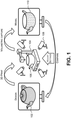
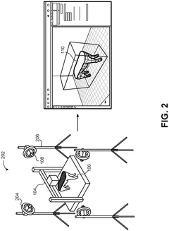
Adjusting manufacturing parameters using artificial intelligence
PatentPendingEP4610028A1
Innovation
- Implementing real-time volumetric video capture and machine learning to compare the printed object with the original design, automatically detecting defects and adjusting manufacturing parameters to eliminate or reduce them.
Materials Science Advancements for Electronic Components
The evolution of materials science has been pivotal in advancing volumetric 3D printing capabilities for electronic components. Traditional electronic manufacturing has relied on rigid substrates and conventional conductive materials, but recent breakthroughs in material development have expanded possibilities for creating complex, high-performance electronic devices through volumetric fabrication techniques.
Photopolymer resins with embedded conductive nanoparticles represent a significant advancement, allowing for single-step printing of functional electronic components. These materials combine the structural integrity of polymers with the electrical conductivity necessary for electronic applications. Silver, copper, and carbon-based nanomaterials have emerged as primary conductivity enhancers, each offering distinct advantages in terms of conductivity, cost, and processing requirements.
Ceramic-polymer composites have gained prominence for their exceptional thermal stability and electrical insulation properties. These materials enable the creation of high-temperature resistant components essential for power electronics and microdevices operating in demanding environments. The integration of piezoelectric ceramics into printable formulations has further expanded functionality, allowing for the fabrication of sensors and actuators directly within printed structures.
Semiconductor-grade materials compatible with volumetric printing processes represent perhaps the most challenging yet promising frontier. Recent developments in photocurable silicon-based resins and germanium compounds have demonstrated potential for creating semiconductor components with acceptable performance characteristics. These materials enable the integration of active electronic elements within a single printing process, reducing assembly steps and enhancing device miniaturization.
Flexible and stretchable electronic materials constitute another critical advancement. By incorporating elastomeric polymers with conductive networks that maintain connectivity under deformation, researchers have developed printable formulations that can produce flexible circuits, wearable sensors, and conformable electronic interfaces. These materials typically employ silver nanowires, liquid metal alloys, or carbon nanotubes arranged in patterns that accommodate mechanical strain.
Multi-material printing capabilities have evolved significantly, allowing for the simultaneous deposition of structural, conductive, and insulating materials within a single fabrication process. This advancement enables the creation of fully functional electronic devices without additional assembly steps. Gradient materials that feature controlled transitions between different electrical, thermal, or mechanical properties further enhance design flexibility and performance optimization.
Biocompatible electronic materials represent an emerging category critical for medical applications. These formulations combine electrical functionality with compatibility for in-vivo use, enabling the creation of implantable sensors, neural interfaces, and drug delivery systems through volumetric printing techniques.
Scalability and Industrial Implementation Strategies
Scaling volumetric 3D printing technology from laboratory demonstrations to industrial applications represents a critical challenge for the widespread adoption of this manufacturing approach in high-performance electronics and micro-device production. Current volumetric printing systems typically operate at laboratory scales with build volumes ranging from a few cubic centimeters to tens of cubic centimeters, which limits their industrial viability.
The transition to industrial-scale implementation requires significant advancements in several key areas. First, scaling the optical systems to accommodate larger build volumes while maintaining high resolution presents substantial engineering challenges. This includes developing more powerful light sources, advanced optical arrangements, and precise control systems capable of maintaining uniform energy distribution throughout larger volumes of photosensitive materials.
Material development represents another crucial aspect of scalability. Current photopolymer resins must be reformulated to maintain consistent curing properties throughout larger volumes while incorporating functional electronic materials. This necessitates careful balancing of photoinitiator concentrations, light absorption characteristics, and viscosity profiles to ensure uniform solidification across increased dimensions.
From a production perspective, implementing volumetric 3D printing in industrial settings requires integration with existing manufacturing workflows. This includes developing standardized interfaces for CAD/CAM systems, establishing quality control protocols, and creating process monitoring tools specific to volumetric fabrication methods. Real-time monitoring systems using embedded sensors or optical feedback mechanisms will be essential for maintaining quality in scaled production environments.
Economic considerations also play a vital role in industrial implementation. Cost models must account for initial equipment investment, material costs, production speeds, and maintenance requirements. Current analyses suggest that volumetric printing becomes increasingly cost-effective as production volumes increase, particularly for complex geometries that would otherwise require multiple manufacturing steps.
Strategic implementation pathways for industry adoption typically follow a phased approach. Initial deployment often targets high-value, low-volume applications where the unique capabilities of volumetric printing provide clear advantages, such as custom medical devices or specialized aerospace components. As the technology matures and costs decrease, applications can expand to broader consumer electronics markets and higher-volume production scenarios.
Collaborative ecosystems involving material suppliers, equipment manufacturers, software developers, and end-users will accelerate industrial implementation. Open innovation platforms and industry consortia have already begun establishing standards and best practices for volumetric printing technologies, which will facilitate wider adoption across multiple sectors requiring high-performance electronic components and micro-devices.
Unlock deeper insights with Patsnap Eureka Quick Research — get a full tech report to explore trends and direct your research. Try now!
Generate Your Research Report Instantly with AI Agent
Supercharge your innovation with Patsnap Eureka AI Agent Platform!