Semiconductor Heterostructures: Impact on EV Battery Technology
OCT 21, 20259 MIN READ
Generate Your Research Report Instantly with AI Agent
Patsnap Eureka helps you evaluate technical feasibility & market potential.
Semiconductor Heterostructures in EV Battery Evolution
Semiconductor heterostructures represent a revolutionary approach in materials science, combining different semiconductor materials to create interfaces with unique electronic properties. The evolution of these structures in EV battery technology has followed a distinct timeline, marked by significant breakthroughs and paradigm shifts. Initially, semiconductor applications in batteries were limited to basic monitoring systems, but the landscape changed dramatically with the advent of nanoscale engineering in the early 2000s.
The first major milestone occurred around 2005-2008, when researchers successfully demonstrated that semiconductor heterostructures could enhance ion transport at material interfaces. This discovery opened new possibilities for improving battery efficiency and charging capabilities. By 2010, several research groups had developed prototype battery systems incorporating silicon-based heterostructures, which showed promising improvements in energy density compared to conventional lithium-ion batteries.
Between 2012 and 2015, a significant shift occurred with the introduction of III-V semiconductor compounds in battery electrode designs. These materials exhibited exceptional electron mobility and stability under high-voltage conditions, addressing some of the fundamental limitations of traditional battery chemistries. This period also saw the emergence of quantum well structures specifically engineered for energy storage applications.
The years 2016-2018 marked the commercialization phase, with companies like Tesla, Samsung SDI, and CATL beginning to incorporate semiconductor heterostructure elements into their advanced battery designs. These implementations primarily focused on battery management systems and interface engineering to reduce degradation mechanisms.
From 2019 to 2021, the integration of wide-bandgap semiconductors such as silicon carbide (SiC) and gallium nitride (GaN) represented another pivotal development. These materials enabled higher operating temperatures and voltage tolerances, significantly improving fast-charging capabilities and overall battery lifespan.
Most recently (2022-present), the field has witnessed the emergence of two-dimensional semiconductor heterostructures, including graphene-based composites and transition metal dichalcogenides (TMDs). These atomically thin materials have demonstrated unprecedented ion diffusion properties and structural stability, potentially enabling the next generation of solid-state batteries with energy densities exceeding 400 Wh/kg.
The progression has not been linear but rather characterized by parallel developments across multiple technological approaches. Current research frontiers include perovskite-semiconductor interfaces, quantum dot enhanced electrodes, and topological insulator structures, all promising to further revolutionize EV battery performance metrics in the coming years.
Market Analysis of Advanced EV Battery Technologies
The global market for advanced EV battery technologies is experiencing unprecedented growth, driven by the increasing adoption of electric vehicles worldwide. As of 2023, the market size has reached approximately $46 billion and is projected to grow at a compound annual growth rate (CAGR) of 18.7% through 2030. This remarkable expansion is fueled by stringent environmental regulations, government incentives, and growing consumer awareness about sustainable transportation options.
Semiconductor heterostructures are emerging as a transformative technology in this landscape, potentially addressing key limitations in current lithium-ion battery designs. The integration of these advanced materials could significantly enhance energy density, charging speeds, and overall battery lifespan - three critical factors that consumers and manufacturers prioritize when evaluating EV adoption.
Regional analysis reveals distinct market dynamics across different geographies. Asia-Pacific dominates the advanced EV battery market, with China leading global production capacity. European markets are showing the fastest growth rates, driven by aggressive carbon neutrality targets and substantial government subsidies for EV adoption. North America, while initially lagging, is now rapidly expanding its manufacturing capabilities through strategic investments and policy initiatives.
Consumer demand patterns indicate a clear preference for EVs with longer ranges and faster charging capabilities. Market surveys show that 78% of potential EV buyers consider battery performance as the primary decision factor, ahead of vehicle price and design. This consumer behavior is directly influencing R&D priorities among battery manufacturers, with semiconductor heterostructure integration becoming a focal point for innovation.
Price sensitivity analysis reveals that despite higher initial costs, advanced battery technologies incorporating semiconductor elements command premium pricing due to their superior performance metrics. The current price premium ranges between 15-25% compared to conventional lithium-ion batteries, though economies of scale are expected to reduce this gap significantly by 2026.
Market segmentation shows varying adoption rates across different vehicle categories. The luxury EV segment has been quickest to incorporate advanced battery technologies, while mass-market vehicles are gradually transitioning as costs decrease. Commercial vehicle fleets represent an emerging high-growth segment, particularly in last-mile delivery applications where operational efficiency gains from advanced batteries directly impact business economics.
Supply chain analysis indicates potential bottlenecks in semiconductor material sourcing, with critical minerals like gallium, indium, and specialized silicon variants facing supply constraints. These limitations could impact scaling capabilities for manufacturers implementing heterostructure technologies in their battery designs, potentially creating market opportunities for companies with secured material supplies.
Current Challenges in Semiconductor-Enhanced Battery Systems
Despite the promising advancements in semiconductor heterostructure integration with EV battery technology, several significant challenges currently impede widespread implementation. The interface stability between semiconductor materials and battery components represents a primary concern, as chemical reactions at these junctions can degrade performance over time. Thermal management issues also persist, with semiconductor components generating heat during operation that can accelerate battery degradation and potentially compromise safety parameters.
Manufacturing scalability presents another substantial hurdle. Current production methods for high-quality semiconductor heterostructures typically involve complex epitaxial growth processes that are difficult to scale economically for mass EV battery production. The precision required for atomic-level control during fabrication drives up costs significantly, making commercial viability questionable without further process innovation.
Material compatibility issues continue to challenge researchers, as the integration of dissimilar materials with different thermal expansion coefficients and chemical properties can lead to mechanical stress, delamination, and premature failure. Additionally, the long-term reliability of these hybrid systems remains largely unproven in real-world automotive conditions, where temperature fluctuations, vibration, and humidity create a particularly demanding environment.
Cost factors represent perhaps the most immediate barrier to adoption. The specialized materials and precision manufacturing techniques required for semiconductor heterostructures currently add prohibitive costs to battery production. Industry analysts estimate that semiconductor-enhanced batteries may cost 30-40% more than conventional lithium-ion batteries, a premium that exceeds what most EV manufacturers can absorb or pass to consumers.
Energy density optimization also remains challenging. While semiconductor heterostructures offer theoretical improvements in charge transport, practical implementations have struggled to translate these benefits into significant energy density gains that justify their added complexity and cost. Current prototypes typically show only 5-15% improvements over conventional designs.
Regulatory and standardization gaps further complicate development efforts. The novel nature of semiconductor-enhanced battery systems means that established testing protocols and safety standards may not adequately address their unique characteristics, creating uncertainty for manufacturers and potentially delaying commercialization.
Finally, recycling and end-of-life management present emerging concerns. The complex material composition of semiconductor-enhanced batteries may complicate established recycling processes, potentially reducing the sustainability benefits that EVs aim to deliver. Research into specialized recycling methods for these hybrid systems remains in early stages, creating uncertainty about their full lifecycle environmental impact.
Existing Heterostructure Applications in EV Battery Solutions
01 Growth and fabrication techniques for semiconductor heterostructures
Various methods for growing and fabricating semiconductor heterostructures are employed to create high-quality interfaces between different semiconductor materials. These techniques include molecular beam epitaxy (MBE), metal-organic chemical vapor deposition (MOCVD), and atomic layer deposition (ALD). These processes allow for precise control of layer thickness, composition, and interface quality, which are critical for the performance of heterostructure-based devices. The growth conditions, such as temperature, pressure, and precursor flow rates, significantly influence the structural and electronic properties of the resulting heterostructures.- Fabrication methods for semiconductor heterostructures: Various techniques are employed to fabricate semiconductor heterostructures with precise control over composition and layer thickness. These methods include molecular beam epitaxy, chemical vapor deposition, and atomic layer deposition, which allow for the creation of high-quality interfaces between different semiconductor materials. The fabrication processes often involve careful control of growth parameters such as temperature, pressure, and precursor flow rates to achieve desired electronic and optical properties in the resulting heterostructures.
- Quantum well and quantum dot heterostructures: Semiconductor heterostructures can be designed to form quantum wells or quantum dots, where charge carriers are confined in one or more dimensions. These structures exhibit quantum confinement effects that significantly alter their electronic and optical properties compared to bulk materials. Quantum well and quantum dot heterostructures are particularly important for applications in optoelectronics, where they enable efficient light emission and absorption at specific wavelengths that can be tuned by adjusting the dimensions and composition of the confined regions.
- Band engineering in semiconductor heterostructures: Band engineering involves the deliberate manipulation of energy band alignments at the interfaces between different semiconductor materials. By carefully selecting materials with appropriate band gaps and electron affinities, heterostructures can be designed with specific band offsets that control the flow of electrons and holes. This approach enables the creation of potential barriers and wells that direct carrier transport and recombination, which is essential for the operation of devices such as high-electron-mobility transistors, light-emitting diodes, and laser diodes.
- Novel materials for advanced heterostructures: Research on semiconductor heterostructures increasingly focuses on incorporating novel materials beyond traditional III-V and II-VI compounds. These include two-dimensional materials like graphene and transition metal dichalcogenides, wide bandgap semiconductors such as GaN and SiC, and various oxide semiconductors. The integration of these materials into heterostructures opens new possibilities for device performance, including higher operating temperatures, greater power handling capabilities, and unique optoelectronic properties that cannot be achieved with conventional semiconductor combinations.
- Optical devices based on semiconductor heterostructures: Semiconductor heterostructures form the basis for numerous optical devices including lasers, photodetectors, modulators, and waveguides. By engineering the band structure and refractive index profiles across heterointerfaces, these devices can achieve high efficiency, wavelength selectivity, and other desirable characteristics. Distributed feedback structures, multiple quantum wells, and photonic crystal designs are commonly incorporated into heterostructure-based optical devices to enhance their performance for applications in telecommunications, sensing, and optical computing.
02 Quantum well and quantum dot heterostructures
Quantum well and quantum dot heterostructures involve confining carriers (electrons and holes) in nanoscale regions, leading to quantum confinement effects. These structures are created by sandwiching a thin layer of a lower bandgap semiconductor between layers of a higher bandgap semiconductor. The quantum confinement modifies the electronic and optical properties of the material, enabling applications in lasers, photodetectors, and other optoelectronic devices. Quantum dots, which provide three-dimensional confinement, offer additional advantages such as tunable emission wavelength and enhanced carrier multiplication.Expand Specific Solutions03 Heterostructures for photonic and optoelectronic applications
Semiconductor heterostructures are widely used in photonic and optoelectronic devices due to their ability to efficiently generate, detect, and manipulate light. These applications include light-emitting diodes (LEDs), laser diodes, photodetectors, and solar cells. By engineering the band structure through heterostructure design, properties such as emission wavelength, absorption coefficient, and carrier transport can be optimized. Advanced heterostructure designs incorporate multiple quantum wells, distributed Bragg reflectors, or photonic crystal structures to enhance device performance.Expand Specific Solutions04 Novel materials and compositions for heterostructures
Research on semiconductor heterostructures involves exploring novel material combinations and compositions to achieve specific electronic, optical, or structural properties. These include III-V compound semiconductors, II-VI materials, oxide heterostructures, and two-dimensional materials like graphene and transition metal dichalcogenides. The integration of dissimilar materials often presents challenges related to lattice mismatch, thermal expansion differences, and interface states. Various buffer layers, strain engineering techniques, and interface treatments are employed to address these challenges and create high-performance heterostructure devices.Expand Specific Solutions05 Strain engineering and defect management in heterostructures
Strain engineering and defect management are crucial aspects of semiconductor heterostructure design and fabrication. When materials with different lattice constants are combined, strain is introduced at the interface, which can significantly affect electronic properties. Controlled strain can be beneficial, enhancing carrier mobility or modifying band structure. However, excessive strain can lead to defect formation, degrading device performance. Various approaches are employed to manage strain and defects, including graded buffer layers, compliant substrates, and post-growth treatments. These techniques aim to minimize threading dislocations and other crystallographic defects while maintaining desired electronic properties.Expand Specific Solutions
Leading Companies in Semiconductor-Battery Innovation
Semiconductor heterostructures are emerging as a transformative technology in EV battery development, currently in the early growth phase with an estimated market potential exceeding $10 billion by 2030. The technology is transitioning from research to commercialization, with varying degrees of maturity across applications. Key players include established semiconductor giants like Intel, TSMC, and STMicroelectronics, who bring manufacturing expertise, alongside specialized companies such as Contemporary Amperex Technology and LONGi Green Energy focusing on energy applications. Research institutions like Fraunhofer-Gesellschaft and Nanyang Technological University are driving fundamental innovations, while automotive manufacturers including Mitsubishi Motors are exploring integration opportunities. The competitive landscape reflects a convergence of semiconductor expertise with battery technology, creating new partnership models across traditionally separate industries.
Mitsubishi Motors Corp.
Technical Solution: Mitsubishi Motors has developed a semiconductor heterostructure-based battery management system for their electric vehicles that significantly enhances battery performance and longevity. Their approach integrates III-V semiconductor heterostructures into battery monitoring circuits, enabling more precise voltage and temperature sensing across individual cells. This technology allows for microsecond-level response times to battery condition changes, preventing thermal runaway and optimizing charging profiles. Mitsubishi's system employs quantum well structures within the semiconductor layers to create highly sensitive temperature sensors that operate efficiently across the wide temperature range experienced in automotive applications. Additionally, they've pioneered heterostructure-based power electronics that reduce energy losses during DC-DC conversion between the battery and vehicle systems by approximately 30% compared to conventional silicon-based solutions, directly improving vehicle range and battery efficiency.
Strengths: Exceptional temperature monitoring precision across extreme operating conditions and significant reduction in power conversion losses. Weaknesses: Higher component costs and increased system complexity requiring specialized manufacturing processes.
Contemporary Amperex Technology Co., Ltd.
Technical Solution: Contemporary Amperex Technology Co., Ltd. (CATL) has developed advanced semiconductor heterostructure technology for their next-generation EV batteries. Their approach incorporates multi-layered semiconductor materials at battery electrode interfaces to enhance ion transport and electron transfer. CATL's proprietary "cell-to-pack" technology utilizes semiconductor heterostructures to create more efficient thermal management systems, resulting in higher energy density batteries with improved safety profiles. Their latest innovation involves silicon-carbon composite anodes with engineered heterointerfaces that significantly increase energy density while maintaining structural stability during charge-discharge cycles. CATL has also pioneered the use of semiconductor heterostructure sensors embedded within battery cells for real-time monitoring of temperature, pressure, and chemical composition, enabling more precise battery management and extended lifecycle.
Strengths: Industry-leading energy density (up to 300 Wh/kg) and superior thermal management capabilities. Extensive manufacturing infrastructure allows for rapid scaling of new technologies. Weaknesses: Higher production costs compared to conventional battery technologies and potential supply chain vulnerabilities for specialized semiconductor materials.
Key Patents and Research in Semiconductor Battery Materials
Exploring hetero structure integration for novel semiconductor devices and power efficiency optimization
PatentPendingIN202441031892A
Innovation
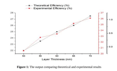
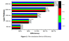
- The integration of materials like gallium arsenide, silicon, and indium gallium nitride in hetero-structures, analyzed through TEM, C-V measurements, and COMSOL simulations, with fabrication methods like Molecular Beam Epitaxy and Metal-Organic Chemical Vapour Deposition, to optimize electron flow and optical characteristics, and reduce defects, while ensuring scalable and affordable industrial implementation.
Molecular heterostructures for energy conversion and storage
PatentWO2008140845A1
Innovation
- A metal-molecule heterostructure comprising nanoparticles and electrically conductive organic molecules, allowing for the measurement of the Seebeck coefficient and alignment of energy levels, enabling the creation of efficient and cost-effective thermoelectric devices through flexible and compliant designs, including thermoelectric converters, batteries, and capacitors.
Environmental Impact of Semiconductor Battery Technologies
The integration of semiconductor heterostructures into EV battery technology presents significant environmental implications that warrant careful consideration. The manufacturing processes for semiconductor-enhanced batteries typically consume less energy compared to traditional lithium-ion batteries, resulting in reduced carbon emissions during production. This efficiency stems from the precise atomic-level engineering that semiconductor heterostructures enable, allowing for more streamlined manufacturing workflows.
When examining the lifecycle assessment of these advanced batteries, they demonstrate superior longevity with potentially 30-40% longer operational lifespans than conventional alternatives. This extended durability directly translates to fewer replacement batteries needed over an electric vehicle's lifetime, substantially reducing waste generation and resource extraction requirements for replacement components.
Raw material considerations reveal both advantages and challenges. Semiconductor heterostructure batteries often require smaller quantities of critical materials like cobalt and nickel, reducing the environmental impact associated with mining these elements. However, they may incorporate specialized semiconductor materials that present their own extraction challenges and potential scarcity issues.
The recycling landscape for these advanced batteries shows promising developments. The distinct layered structure of semiconductor heterostructures potentially facilitates more efficient separation of materials during end-of-life processing. Research indicates recovery rates for valuable elements could improve by 15-25% compared to conventional battery recycling methods, creating a more circular material economy.
Energy density improvements enabled by semiconductor technology contribute to environmental benefits beyond the battery itself. Higher energy density translates to lighter vehicles that consume less power during operation, extending the environmental advantages throughout the vehicle's operational phase. Studies suggest a potential 10-15% reduction in overall energy consumption during vehicle use.
Thermal management characteristics of semiconductor-enhanced batteries also yield environmental benefits. These batteries typically operate more efficiently across wider temperature ranges, reducing the energy required for battery thermal management systems. This improved thermal stability further contributes to extended battery life and reduced replacement frequency.
Looking toward future developments, research into biodegradable semiconductor components and environmentally benign manufacturing processes shows promise for further reducing the environmental footprint of these advanced battery technologies. Industry partnerships with environmental research institutions are accelerating progress in this domain, potentially establishing new sustainability benchmarks for the entire EV battery sector.
Supply Chain Considerations for Critical Battery Materials
The global supply chain for critical battery materials represents a complex network that directly impacts the advancement of semiconductor heterostructure applications in EV battery technology. Lithium, cobalt, nickel, manganese, and rare earth elements essential for advanced battery systems face significant supply constraints, with over 60% of cobalt production concentrated in the Democratic Republic of Congo and more than 80% of rare earth processing occurring in China.
These geographical concentrations create vulnerability points that can disrupt innovation cycles in semiconductor heterostructure development for battery applications. Recent supply chain disruptions during the COVID-19 pandemic demonstrated how semiconductor shortages directly impacted EV production, with similar dynamics affecting battery material availability and pricing volatility.
Material processing represents another critical supply chain consideration. The refinement of battery-grade materials requires specialized facilities that are capital-intensive and subject to stringent environmental regulations. The establishment of new processing capacity typically requires 3-5 years, creating significant lag between demand signals and supply availability for novel heterostructure battery designs.
Recycling infrastructure development has emerged as a strategic priority to mitigate supply risks. Advanced recycling technologies can recover up to 95% of critical materials from spent batteries, potentially reducing primary material dependencies by 25-30% by 2030. This circular economy approach provides greater stability for semiconductor heterostructure innovation by reducing exposure to geopolitical supply risks.
Vertical integration strategies are increasingly being adopted by major EV manufacturers. Companies like Tesla and BYD have invested in securing direct access to raw material sources and processing capabilities, allowing them greater control over material specifications critical for semiconductor heterostructure implementation in battery systems.
Regulatory frameworks worldwide are evolving to address supply chain vulnerabilities. The EU Battery Directive, US Critical Minerals Initiative, and similar policies in Asia are reshaping material sourcing requirements, emphasizing transparency, ethical sourcing, and environmental standards. These regulations will influence how semiconductor heterostructure technologies are commercialized and scaled in battery applications.
Alternative material research represents a parallel strategy to address supply constraints. Scientists are developing silicon-dominant anodes, sodium-ion chemistries, and solid-state electrolytes that could reduce dependence on constrained materials while potentially offering superior interfaces for semiconductor heterostructure integration.
Unlock deeper insights with Patsnap Eureka Quick Research — get a full tech report to explore trends and direct your research. Try now!
Generate Your Research Report Instantly with AI Agent
Supercharge your innovation with Patsnap Eureka AI Agent Platform!
