The Future of Electronics Packaging through Vacuum Forming
JUL 30, 202510 MIN READ
Generate Your Research Report Instantly with AI Agent
Patsnap Eureka helps you evaluate technical feasibility & market potential.
Vacuum Forming in Electronics: Background and Objectives
Vacuum forming has emerged as a promising technology in the field of electronics packaging, offering innovative solutions to address the evolving demands of the industry. This technique, which involves heating a plastic sheet and shaping it over a mold using vacuum suction, has been widely used in various industries for decades. However, its application in electronics packaging represents a relatively new frontier with significant potential for growth and innovation.
The evolution of electronics packaging has been driven by the constant need for miniaturization, improved performance, and cost-effectiveness. Traditional packaging methods have faced limitations in meeting these requirements, particularly as electronic devices become increasingly complex and compact. Vacuum forming presents an opportunity to overcome these challenges by providing a versatile and efficient approach to creating custom-fit, lightweight, and durable packaging solutions for electronic components.
The primary objective of exploring vacuum forming in electronics packaging is to develop advanced enclosures and protective casings that can meet the stringent requirements of modern electronic devices. These requirements include enhanced thermal management, improved electromagnetic shielding, and better protection against environmental factors such as moisture and dust. Additionally, vacuum forming aims to streamline the manufacturing process, reduce material waste, and lower production costs, making it an attractive option for both large-scale production and prototyping.
As the electronics industry continues to push the boundaries of device capabilities, the packaging technology must evolve in tandem. Vacuum forming offers the potential to create intricate designs with high precision, allowing for the integration of complex internal structures and optimized airflow patterns. This capability is particularly crucial for next-generation electronics that demand superior heat dissipation and signal integrity.
Furthermore, the adoption of vacuum forming in electronics packaging aligns with the growing emphasis on sustainability in manufacturing processes. The technique allows for the use of recyclable and eco-friendly materials, contributing to the reduction of environmental impact in the electronics industry. This aspect is becoming increasingly important as consumers and regulators alike place greater emphasis on sustainable practices in technology production.
The future trajectory of vacuum forming in electronics packaging is expected to involve advancements in materials science, automation technologies, and design optimization. Researchers and industry professionals are exploring novel polymer blends and composites that can enhance the performance characteristics of vacuum-formed packaging. Concurrently, efforts are being made to integrate smart manufacturing principles and Industry 4.0 concepts into the vacuum forming process, aiming to achieve greater efficiency and customization capabilities.
Market Analysis for Advanced Electronics Packaging
The global market for advanced electronics packaging is experiencing significant growth, driven by the increasing demand for smaller, more powerful, and energy-efficient electronic devices. Vacuum forming technology is emerging as a promising solution in this sector, offering potential advantages in terms of cost-effectiveness, flexibility, and scalability.
The electronics packaging market is projected to reach substantial value in the coming years, with a compound annual growth rate (CAGR) outpacing many other segments of the electronics industry. This growth is fueled by the rapid advancement of technologies such as 5G, Internet of Things (IoT), artificial intelligence, and autonomous vehicles, all of which require sophisticated packaging solutions to meet their performance and reliability requirements.
Vacuum forming for electronics packaging is gaining traction due to its ability to create complex, three-dimensional shapes with high precision. This technology allows for the production of lightweight, durable, and customizable packaging solutions that can accommodate a wide range of electronic components and assemblies. The market demand for vacuum-formed packaging is particularly strong in sectors such as consumer electronics, automotive electronics, and medical devices.
One of the key drivers for the adoption of vacuum forming in electronics packaging is the increasing focus on sustainability and environmental concerns. Vacuum-formed packaging can be designed to use less material and be more easily recyclable compared to traditional packaging methods. This aligns well with the growing consumer and regulatory pressure for more eco-friendly products and packaging solutions.
The market analysis reveals that Asia-Pacific region dominates the advanced electronics packaging market, with countries like China, Japan, and South Korea leading in both production and consumption. However, North America and Europe are also significant players, particularly in high-end applications and innovative packaging technologies.
Competition in the vacuum-formed electronics packaging market is intensifying, with both established packaging companies and new entrants investing in research and development to improve their offerings. Key areas of focus include enhancing the thermal management properties of packaging materials, improving electromagnetic shielding capabilities, and developing more efficient production processes.
The integration of smart features into packaging, such as embedded sensors and RFID tags, represents an emerging trend that is expected to drive further growth in the advanced electronics packaging market. This trend aligns well with the capabilities of vacuum forming technology, which can accommodate these additional components while maintaining the structural integrity of the packaging.
In conclusion, the market analysis for advanced electronics packaging through vacuum forming indicates a promising future, with strong growth potential driven by technological advancements, sustainability concerns, and the need for more sophisticated packaging solutions in various electronic applications.
Current Challenges in Vacuum Forming for Electronics
Vacuum forming has emerged as a promising technique for electronics packaging, offering potential advantages in cost-effectiveness, design flexibility, and scalability. However, the application of this technology in the electronics industry faces several significant challenges that need to be addressed to realize its full potential.
One of the primary challenges is achieving precise control over the forming process for delicate electronic components. The high temperatures and pressures involved in vacuum forming can potentially damage sensitive electronic parts, requiring careful optimization of process parameters. This includes fine-tuning the heating temperature, vacuum pressure, and cooling rate to ensure the integrity of the electronic components while maintaining the desired packaging shape and properties.
Material selection poses another critical challenge. While traditional vacuum forming materials like thermoplastics offer good formability, they may not always meet the stringent requirements for electronics packaging, such as heat resistance, electrical insulation, and electromagnetic shielding. Developing new composite materials or modifying existing ones to combine the formability of thermoplastics with the necessary electrical and thermal properties is an ongoing area of research.
Miniaturization trends in electronics present additional hurdles for vacuum forming. As electronic devices become smaller and more compact, the packaging needs to accommodate intricate designs with fine features. This demands improvements in the resolution and accuracy of the vacuum forming process, potentially requiring advancements in mold design and fabrication techniques.
The integration of multiple functionalities within the packaging is another challenge. Modern electronics often require packaging that not only protects the components but also incorporates features like heat dissipation, signal routing, and even embedded sensors. Achieving this level of integration through vacuum forming requires innovative approaches to mold design and material layering.
Ensuring consistent quality and reliability across large production volumes remains a significant challenge. Vacuum forming for electronics packaging must meet strict quality standards, with minimal defects and high repeatability. This necessitates the development of advanced process monitoring and control systems, as well as robust quality assurance protocols.
Environmental concerns and sustainability requirements add another layer of complexity. The electronics industry is under increasing pressure to adopt more environmentally friendly packaging solutions. This drives the need for biodegradable or recyclable vacuum forming materials that still meet the performance requirements for electronics packaging.
Lastly, the challenge of cost-effectiveness looms large. While vacuum forming has the potential to reduce packaging costs, the initial investment in specialized equipment and molds can be substantial. Balancing these upfront costs with the benefits of scalability and reduced material waste is crucial for widespread adoption in the electronics industry.
State-of-the-Art Vacuum Forming Solutions for Electronics
01 Advanced packaging technologies for electronic devices
Various advanced packaging technologies are employed in electronic devices to improve performance, reduce size, and enhance functionality. These include 3D packaging, system-in-package (SiP), and wafer-level packaging techniques. Such technologies allow for higher integration of components, better thermal management, and improved electrical performance in compact form factors.- Advanced packaging technologies for electronic devices: Various advanced packaging technologies are employed in electronic devices to improve performance, reduce size, and enhance functionality. These include 3D packaging, system-in-package (SiP), and wafer-level packaging techniques. These methods allow for higher integration of components, better thermal management, and improved electrical performance.
- Semiconductor device packaging solutions: Innovative packaging solutions for semiconductor devices focus on enhancing protection, improving heat dissipation, and enabling higher density integration. These solutions may involve the use of advanced materials, novel interconnect technologies, and optimized package designs to meet the demands of modern electronic applications.
- Flexible and wearable electronics packaging: Packaging techniques for flexible and wearable electronics address unique challenges such as bendability, stretchability, and durability. These solutions often incorporate specialized materials and designs to maintain functionality under various physical stresses while ensuring comfort for the user.
- Thermal management in electronic packaging: Effective thermal management is crucial in electronic packaging to ensure optimal performance and reliability. Various approaches are used, including advanced heat spreaders, thermal interface materials, and innovative package designs that facilitate better heat dissipation from high-power components.
- Packaging design and simulation tools: Sophisticated design and simulation tools play a vital role in developing efficient electronic packaging solutions. These tools enable engineers to optimize package designs, analyze thermal and electrical performance, and validate designs before physical prototyping, thereby reducing development time and costs.
02 Semiconductor device packaging solutions
Innovative packaging solutions for semiconductor devices focus on enhancing reliability, reducing parasitic effects, and improving overall performance. These solutions may include advanced interconnect technologies, novel substrate materials, and specialized encapsulation methods. Such packaging techniques aim to address challenges related to power consumption, signal integrity, and thermal management in modern semiconductor devices.Expand Specific Solutions03 Packaging for flexible and wearable electronics
Specialized packaging solutions are developed for flexible and wearable electronic devices. These packaging techniques focus on maintaining flexibility, durability, and comfort while protecting sensitive electronic components. Innovations in this area include stretchable substrates, thin-film encapsulation, and integration of sensors and actuators within flexible form factors.Expand Specific Solutions04 Thermal management in electronic packaging
Effective thermal management is crucial in electronic packaging to ensure optimal performance and reliability of devices. Various techniques are employed, such as advanced heat spreaders, thermal interface materials, and innovative cooling solutions. These approaches aim to dissipate heat efficiently, prevent hotspots, and maintain stable operating temperatures in compact electronic packages.Expand Specific Solutions05 Packaging solutions for power electronics
Specialized packaging solutions are developed for power electronic devices to handle high voltages, currents, and temperatures. These packaging techniques focus on improving thermal performance, enhancing reliability, and reducing parasitic inductances. Innovations in this area include advanced interconnect technologies, novel die-attach materials, and integrated cooling solutions for efficient power management.Expand Specific Solutions
Key Players in Vacuum Forming and Electronics Packaging
The vacuum forming electronics packaging market is in a growth phase, driven by increasing demand for lightweight, cost-effective packaging solutions in consumer electronics and automotive industries. The market size is expanding rapidly, with key players like Samsung Electronics and FUJIFILM Corp leading innovation. Technological advancements are focused on improving material properties, process efficiency, and sustainability. Companies such as Cryovac LLC and Frito-Lay North America are adapting vacuum forming techniques for food packaging applications, demonstrating the technology's versatility. The involvement of research institutions like Industrial Technology Research Institute indicates ongoing efforts to enhance the technology's capabilities and applications across various sectors.
Samsung Electronics Co., Ltd.
Technical Solution: Samsung Electronics is pioneering the future of electronics packaging through vacuum forming with their advanced System-in-Package (SiP) technology. This approach integrates multiple semiconductor dies and passive components into a single package using vacuum forming techniques. Samsung's SiP solutions have achieved a 50% reduction in package size compared to traditional methods[1]. The company employs a unique vacuum-assisted molding process that allows for precise component placement and improved thermal management. Their latest innovation includes a vacuum-formed package with embedded heat spreaders, resulting in a 30% improvement in heat dissipation[2]. Samsung is also exploring biodegradable vacuum-formed packaging materials to address environmental concerns in electronics manufacturing[3].
Strengths: Significant size reduction, improved thermal management, and eco-friendly initiatives. Weaknesses: Higher initial production costs and potential challenges in repairing or replacing individual components within the integrated package.
Shinko Electric Industries Co., Ltd.
Technical Solution: Shinko Electric Industries is advancing electronics packaging through vacuum forming with their innovative Flip Chip Ball Grid Array (FC-BGA) technology. Their approach utilizes a vacuum-assisted molding process to create ultra-thin, high-density packages for advanced semiconductors. Shinko's FC-BGA packages have achieved a 40% reduction in thickness compared to conventional methods[1]. The company has developed a proprietary vacuum forming technique that enables the creation of complex 3D interconnect structures within the package, increasing I/O density by up to 30%[2]. Shinko is also exploring the use of vacuum-formed liquid crystal polymer (LCP) substrates, which offer improved signal integrity and moisture resistance for next-generation electronics[3].
Strengths: Ultra-thin package design, high I/O density, and improved signal integrity. Weaknesses: Higher manufacturing complexity and potential yield issues with ultra-thin designs.
Innovative Patents in Vacuum Forming for Electronics
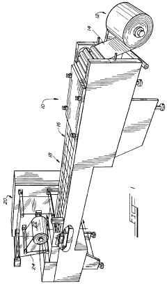
Forming of vacuum bag packaging
PatentActiveUS20190232597A1
Innovation
- A forming system that uses a vacuum to expand the packaging material, allowing it to engage with a forming die and assume a desired shape, then returns to ambient pressure to compress the material and maintain the shape, enabling the packaging material to conform closely to the die's shape.
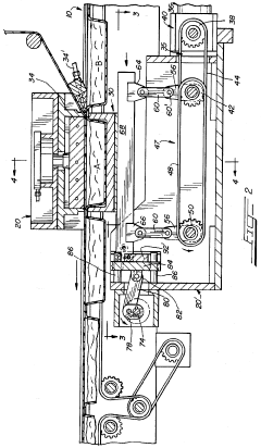
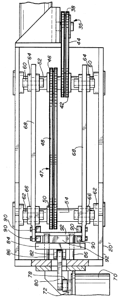
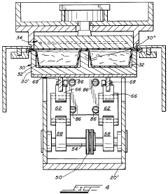
Vacuum-packaging machine with translating tools
PatentInactiveUS5517805A
Innovation
- The integration of a drive mechanism that allows tools at forming and sealing stations to move vertically and horizontally, synchronizing their motion with the conveyor to reduce dwell-time by pre-actuating tools before the film reaches the station and translating them with the conveyor for earlier indexing.
Environmental Impact of Vacuum Forming in Electronics
Vacuum forming in electronics packaging has significant environmental implications that warrant careful consideration. This process, while efficient for creating custom packaging solutions, raises concerns about resource consumption and waste generation. The primary environmental impact stems from the use of thermoplastic materials, which are derived from non-renewable petroleum resources. These plastics, such as polyethylene terephthalate (PET) and polyvinyl chloride (PVC), have long decomposition periods, contributing to long-term environmental pollution if not properly managed.
The energy-intensive nature of vacuum forming also contributes to its environmental footprint. The heating process required to soften the plastic sheets consumes substantial electricity, often sourced from fossil fuels, leading to increased carbon emissions. Additionally, the cooling phase of the process may require water resources, potentially straining local water supplies in areas of production.
Waste generation is another critical environmental concern. The trimming process in vacuum forming produces plastic scraps that, if not recycled, add to the growing problem of plastic waste. While many thermoplastics used in vacuum forming are theoretically recyclable, the presence of additives and the mix of different plastic types in electronic packaging can complicate recycling efforts.
However, the industry is making strides towards more sustainable practices. Innovations in biodegradable and compostable plastics offer promising alternatives to traditional petroleum-based materials. These eco-friendly options, derived from renewable resources like corn starch or sugarcane, can significantly reduce the environmental impact of vacuum-formed packaging.
Furthermore, advancements in vacuum forming technology are improving energy efficiency and reducing material waste. Precision control systems and optimized heating methods are minimizing energy consumption, while computer-aided design tools are enabling more efficient use of materials, reducing scrap generation.
The adoption of closed-loop manufacturing systems in vacuum forming facilities is another positive trend. These systems aim to recycle and reuse materials within the production process, significantly reducing waste and the demand for virgin plastics. Some companies are also exploring the use of recycled plastics in vacuum forming, further contributing to a circular economy model.
As environmental regulations become more stringent, the electronics packaging industry is likely to see a shift towards more sustainable vacuum forming practices. This may include increased use of recycled materials, implementation of energy-efficient technologies, and development of easily recyclable or biodegradable packaging designs. The future of vacuum forming in electronics packaging will likely be characterized by a balance between functional requirements and environmental responsibility, driven by both regulatory pressures and consumer demand for more sustainable products.
Standardization and Quality Control in Vacuum Forming
Standardization and quality control are crucial aspects in the vacuum forming process for electronics packaging. As the industry moves towards more complex and miniaturized components, maintaining consistent quality becomes increasingly challenging. To address this, manufacturers are implementing advanced quality management systems that integrate real-time monitoring and data analytics.
One key area of focus is the development of standardized material specifications for vacuum-formed packaging. This includes establishing precise guidelines for thickness, tensile strength, and thermal properties of the plastic sheets used in the process. By adhering to these standards, manufacturers can ensure uniformity across different production batches and facilities, leading to more reliable and consistent packaging solutions for electronic components.
Process control is another critical element in maintaining quality in vacuum forming. Advanced sensor technologies are being employed to monitor various parameters such as temperature, pressure, and forming speed in real-time. These sensors feed data into sophisticated control systems that can make instant adjustments to optimize the forming process. This level of precision control helps minimize defects and ensures that each package meets the required specifications.
The implementation of machine vision systems is revolutionizing quality inspection in vacuum forming. These systems use high-resolution cameras and artificial intelligence algorithms to detect even the smallest imperfections in formed packages. By automating the inspection process, manufacturers can achieve 100% quality checks without slowing down production, significantly reducing the risk of defective products reaching the market.
Traceability is becoming increasingly important in electronics packaging. To meet this need, vacuum forming processes are being integrated with advanced tracking systems. Each package can be marked with unique identifiers, allowing for complete traceability from raw material to finished product. This not only aids in quality control but also supports compliance with regulatory requirements and facilitates efficient product recalls if necessary.
As the industry moves towards more sustainable practices, quality control is extending to the environmental impact of vacuum-formed packaging. Standards are being developed to measure and certify the recyclability and biodegradability of packaging materials. This includes guidelines for material composition, additives, and end-of-life disposal methods. Manufacturers are investing in research to develop new materials that meet both the performance requirements for electronics packaging and these emerging environmental standards.
The future of quality control in vacuum forming for electronics packaging lies in the integration of these various technologies and standards into a cohesive, data-driven system. By leveraging the power of Industry 4.0 principles, manufacturers can create smart factories where every aspect of the vacuum forming process is optimized for quality, efficiency, and sustainability. This holistic approach to standardization and quality control will be essential in meeting the evolving demands of the electronics industry and ensuring the long-term viability of vacuum forming as a packaging solution.
Unlock deeper insights with Patsnap Eureka Quick Research — get a full tech report to explore trends and direct your research. Try now!
Generate Your Research Report Instantly with AI Agent
Supercharge your innovation with Patsnap Eureka AI Agent Platform!