Why Plasma Treatment is Integral to Modern Manufacturing
OCT 14, 20259 MIN READ
Generate Your Research Report Instantly with AI Agent
Patsnap Eureka helps you evaluate technical feasibility & market potential.
Plasma Treatment Evolution and Manufacturing Objectives
Plasma treatment technology has evolved significantly over the past several decades, transforming from a niche scientific process to a fundamental component of modern manufacturing. The journey began in the early 1960s with rudimentary plasma applications primarily in aerospace and specialized electronics. By the 1980s, plasma treatment had expanded into semiconductor fabrication, establishing itself as a critical process for microelectronics manufacturing. The 1990s witnessed further diversification as plasma technologies penetrated automotive, medical device, and consumer electronics industries.
The evolution of plasma treatment has been characterized by continuous improvements in precision, energy efficiency, and process control. Early systems required high power consumption and offered limited treatment uniformity, whereas contemporary plasma systems deliver nanometer-scale precision with significantly reduced energy requirements. This progression has been driven by the increasing demands of miniaturization in electronics, stringent surface quality requirements in medical applications, and sustainability concerns across all manufacturing sectors.
Current technological trends in plasma treatment include atmospheric pressure plasma systems that eliminate the need for vacuum chambers, thereby reducing operational complexity and costs. Additionally, the development of selective plasma treatment capabilities allows manufacturers to modify specific surface areas without affecting adjacent regions, a critical advancement for complex multi-material assemblies. Digital integration and real-time monitoring systems represent another significant trend, enabling precise process control and quality assurance in high-volume production environments.
The primary manufacturing objectives of plasma treatment center around surface modification to enhance adhesion, wettability, and biocompatibility. In electronics manufacturing, plasma treatment creates ultra-clean surfaces essential for reliable bonding and coating adhesion. For medical device production, plasma processes ensure sterility and biocompatibility while enabling precise surface functionalization. In automotive and aerospace applications, plasma treatment facilitates stronger adhesive bonds for composite materials, contributing to lighter, more fuel-efficient vehicles.
Looking forward, the trajectory of plasma treatment technology points toward more sustainable processes with reduced environmental impact, greater integration with automated manufacturing systems, and expanded capabilities for treating complex three-dimensional geometries. The convergence of plasma technology with advanced materials science is expected to yield novel surface properties that enable next-generation products across multiple industries, from flexible electronics to implantable medical devices.
Industrial Market Demand for Plasma Processing
The global market for plasma processing technologies has witnessed substantial growth over the past decade, driven primarily by increasing applications across diverse manufacturing sectors. Current market valuations place the plasma processing equipment industry at approximately $10 billion, with projections indicating a compound annual growth rate of 6-8% through 2028. This growth trajectory reflects the expanding industrial recognition of plasma treatment's critical role in modern manufacturing processes.
Semiconductor fabrication represents the largest market segment for plasma processing, accounting for nearly 40% of total demand. The continuous miniaturization of electronic components, coupled with the industry's push toward 3nm and smaller process nodes, has intensified the need for precise plasma etching and deposition technologies. Major semiconductor manufacturers have increased their capital expenditure on advanced plasma processing equipment by 15-20% annually since 2019.
The medical device manufacturing sector has emerged as another significant growth area, with plasma sterilization and surface modification technologies becoming essential for producing biocompatible implants and diagnostic equipment. Market analysis indicates that plasma-based surface treatments in medical manufacturing have grown at twice the rate of traditional chemical treatments over the past five years, driven by stricter regulatory requirements and enhanced performance characteristics.
Automotive and aerospace industries collectively represent approximately 18% of the plasma processing market, primarily utilizing plasma technologies for surface preparation before coating, bonding, or painting. The transition toward lightweight materials and composite structures in these sectors has further accelerated the adoption of specialized plasma treatments that can effectively modify difficult-to-bond surfaces without thermal damage.
Consumer electronics manufacturers have increasingly incorporated plasma processing into their production lines, particularly for display technologies and protective coatings. The demand for scratch-resistant, water-repellent, and antimicrobial surfaces on consumer devices has created a specialized market segment growing at 10-12% annually.
Textile and packaging industries represent emerging markets for atmospheric plasma treatments, with applications in creating functional fabrics and environmentally friendly packaging materials. These sectors are projected to be the fastest-growing application areas over the next five years, with adoption rates increasing by 25-30% annually from a relatively small base.
Regional analysis reveals Asia-Pacific as the dominant market for plasma processing equipment, accounting for over 45% of global demand, followed by North America and Europe. This distribution closely mirrors the geographic concentration of semiconductor and electronics manufacturing facilities.
Current Plasma Technology Landscape and Challenges
Plasma technology has evolved significantly over the past few decades, establishing itself as a cornerstone in modern manufacturing processes. Currently, the global plasma treatment market is experiencing robust growth, with an estimated value of $2.5 billion in 2022 and projections indicating a compound annual growth rate of 16% through 2030. This expansion reflects the increasing adoption of plasma technologies across diverse industrial sectors.
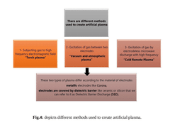
The contemporary plasma technology landscape encompasses several key variants, including atmospheric pressure plasma, low-pressure plasma, vacuum plasma, and corona discharge systems. Each variant offers distinct advantages for specific applications, with atmospheric pressure plasma gaining particular traction due to its operational flexibility and reduced infrastructure requirements compared to vacuum-based systems.
Despite widespread adoption, plasma treatment technologies face several significant challenges. Energy efficiency remains a primary concern, as conventional plasma systems often require substantial power inputs, contributing to high operational costs and environmental impact. Current research indicates that most industrial plasma systems operate at energy efficiency rates between 10-40%, highlighting considerable room for improvement.
Scalability presents another major hurdle, particularly for industries requiring treatment of large or geometrically complex components. While batch processing systems have improved throughput capabilities, continuous inline treatment for high-volume manufacturing remains technically challenging, especially for three-dimensional objects with intricate surface geometries.
Process control and reproducibility constitute additional technical barriers. The plasma state is inherently sensitive to numerous variables including gas composition, pressure, power input, and substrate characteristics. Current monitoring systems often lack the precision required for real-time adjustments, resulting in quality inconsistencies that impact yield rates in precision manufacturing contexts.
Geographically, plasma technology development exhibits notable concentration patterns. North America and Europe, particularly Germany and the United States, maintain leadership in research and development of advanced plasma systems, accounting for approximately 60% of plasma technology patents filed annually. However, Asia-Pacific regions, led by Japan, South Korea, and increasingly China, are rapidly closing this gap, demonstrating accelerated growth in both research output and industrial implementation.
Environmental considerations are emerging as a critical focus area for next-generation plasma technologies. Traditional plasma processes often utilize perfluorinated compounds and other environmentally persistent chemicals. Regulatory pressures, particularly in Europe under REACH legislation, are driving urgent research into more sustainable plasma chemistries and closed-loop systems that minimize environmental footprint while maintaining treatment efficacy.
Contemporary Plasma Treatment Implementation Methods
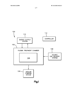
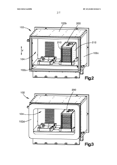
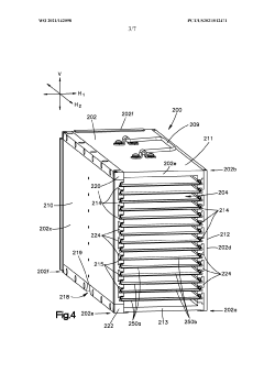
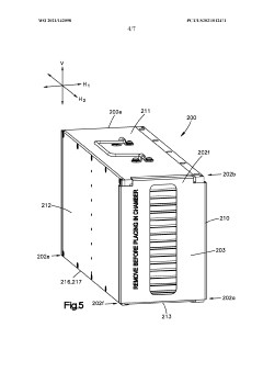
01 Plasma processing chambers and apparatus design
Various designs of plasma processing chambers and apparatus are used for efficient plasma treatment. These designs include specific configurations for plasma generation, distribution, and control within the chamber. Features such as electrode arrangements, gas delivery systems, and chamber geometry are optimized to enhance plasma uniformity and process efficiency. Advanced chamber designs incorporate mechanisms for temperature control, pressure regulation, and plasma confinement to improve treatment results.- Plasma treatment systems for semiconductor processing: Plasma treatment systems are widely used in semiconductor manufacturing for etching, deposition, and surface modification. These systems typically include plasma chambers with specialized electrodes, RF power sources, and gas delivery systems designed to create controlled plasma environments. The technology enables precise processing of semiconductor wafers, allowing for the creation of nanoscale features and structures essential for modern electronic devices.
- Plasma chamber design and configuration: Advanced plasma chamber designs incorporate specific features to optimize treatment uniformity and efficiency. These chambers may include specialized electrode configurations, gas distribution systems, and temperature control mechanisms. Innovations in chamber design focus on improving plasma stability, reducing contamination, and enhancing process control for various applications including semiconductor fabrication, material modification, and thin film deposition.
- Plasma power supply and control systems: Power supply and control systems for plasma treatment equipment involve sophisticated RF generators, impedance matching networks, and feedback control mechanisms. These systems regulate plasma parameters such as power density, frequency, and pulse characteristics to achieve desired treatment outcomes. Advanced control algorithms enable precise manipulation of plasma properties, allowing for customized treatments across various industrial applications.
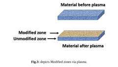
- Surface modification using plasma treatment: Plasma treatment is utilized for modifying surface properties of various materials including polymers, metals, and ceramics. The process can alter surface energy, improve adhesion characteristics, enhance wettability, and create functional groups on surfaces. These modifications enable better bonding, printing, coating, and other secondary processes across industries such as electronics, medical devices, automotive, and textiles.
- Atmospheric pressure plasma treatment techniques: Atmospheric pressure plasma treatment offers advantages over vacuum-based systems by eliminating the need for complex vacuum equipment. These systems operate at normal atmospheric conditions while still providing effective surface modification capabilities. The technology includes dielectric barrier discharge, plasma jets, and corona discharge methods that can be integrated into continuous production lines for treating large areas or complex geometries efficiently.
02 Plasma generation and power control methods
Different methods for generating and controlling plasma are employed in treatment processes. These include RF (radio frequency) power systems, microwave excitation, and pulsed plasma techniques. Power control mechanisms regulate the plasma density, energy, and stability during treatment. Advanced systems incorporate impedance matching networks, frequency tuning, and power modulation to optimize plasma characteristics for specific applications. These methods enable precise control over plasma parameters to achieve desired treatment outcomes.Expand Specific Solutions03 Surface modification and treatment applications
Plasma treatment is widely used for surface modification of various materials. Applications include surface activation, cleaning, etching, and deposition of thin films. The treatment can alter surface properties such as wettability, adhesion, and biocompatibility. Plasma processes are employed in industries ranging from semiconductor manufacturing to medical device production. The controlled modification of surface characteristics enables improved product performance and enables new material functionalities.Expand Specific Solutions04 Semiconductor processing and fabrication techniques
Plasma treatment plays a crucial role in semiconductor processing and fabrication. It is used for etching patterns, removing photoresist, depositing thin films, and cleaning wafer surfaces. Advanced plasma techniques enable the creation of high-aspect-ratio features and precise material removal at nanometer scales. These processes are essential for manufacturing integrated circuits, microelectromechanical systems (MEMS), and other semiconductor devices. Plasma-based fabrication techniques continue to evolve to meet the demands of increasingly complex semiconductor architectures.Expand Specific Solutions05 Atmospheric and low-pressure plasma technologies
Plasma treatment can be performed under different pressure conditions, including atmospheric pressure and low-pressure environments. Atmospheric plasma systems offer advantages such as simplified equipment design and continuous processing capabilities. Low-pressure plasma provides better control over plasma parameters and treatment uniformity. Each approach has specific applications based on material sensitivity, process requirements, and production constraints. Recent developments include hybrid systems that combine benefits of both pressure regimes for enhanced treatment flexibility.Expand Specific Solutions
Leading Manufacturers and Research Institutions in Plasma Industry
Plasma treatment technology has evolved into a critical component of modern manufacturing, currently in a mature growth phase with an estimated market size of $2-3 billion annually and expanding at 6-8% CAGR. The competitive landscape features established industry leaders like Applied Materials, Tokyo Electron, and Lam Research dominating semiconductor applications, while Nordson and SCHOTT serve specialized industrial segments. Recent technological advancements from companies like NAURA Microelectronics and Suzhou OPS Plasma Technology are challenging traditional players, particularly in Asia. IBM and Samsung are driving innovation through research partnerships, focusing on next-generation applications in nanomaterials and flexible electronics, indicating the technology's continued evolution toward more precise, energy-efficient, and versatile plasma treatment solutions.
Tokyo Electron Ltd.
Technical Solution: Tokyo Electron (TEL) has developed the Tactras™ plasma treatment system that employs their proprietary Radial Line Slot Antenna (RLSA) technology to generate high-density, low-temperature plasma for surface modification applications. This innovative approach creates highly uniform plasma across large substrate areas without the need for magnetic confinement, resulting in more consistent treatment outcomes. TEL's plasma systems utilize advanced microwave power delivery (2.45GHz) that enables efficient plasma generation at lower pressures (0.1-10 Pa range), allowing for deeper penetration of plasma effects without thermal damage to sensitive substrates. Their CLEAN TRACK™ LITHIUS Pro™ platform integrates plasma treatment capabilities directly into photolithography track systems, enabling in-line surface preparation that significantly improves adhesion properties and pattern fidelity in semiconductor manufacturing. TEL has also pioneered plasma-assisted atomic layer deposition (PA-ALD) technology in their NT333™ system, which combines precise plasma activation with atomic layer precision for creating ultrathin functional coatings with exceptional conformality and density.
Strengths: Superior plasma uniformity across large substrates (±1.5% variation across 300mm wafers); excellent energy efficiency with up to 30% lower power consumption than conventional RF plasma systems; highly automated operation reducing human error factors. Weaknesses: Higher initial capital investment; specialized maintenance requirements for microwave components; more complex integration with existing manufacturing lines compared to simpler plasma technologies.
Applied Materials, Inc.
Technical Solution: Applied Materials has developed comprehensive plasma treatment solutions centered around their Endura® platform, which utilizes advanced plasma-enhanced physical vapor deposition (PVD) and plasma-enhanced chemical vapor deposition (PECVD) technologies. Their systems employ high-density inductively coupled plasma (ICP) sources that achieve precise control over plasma parameters, enabling uniform treatment across large substrate areas. The company's Producer® platform incorporates dual-frequency capacitively coupled plasma technology that allows independent control of ion energy and plasma density, critical for sensitive surface modifications without substrate damage. Applied Materials has also pioneered remote plasma source (RPS) technology that generates high-density plasma away from the substrate, reducing potential damage while maintaining effective surface activation and cleaning capabilities. Their integrated plasma treatment chambers can be configured for sequential processing without breaking vacuum, significantly enhancing manufacturing efficiency and reducing contamination risks.
Strengths: Industry-leading plasma uniformity across large substrates (>99% uniformity on 300mm wafers); exceptional process control with multi-variable plasma parameter adjustment; seamless integration with other manufacturing steps. Weaknesses: Higher capital investment requirements compared to standalone systems; complex systems require specialized technical expertise for operation and maintenance; customization for unique applications may require significant engineering resources.
Critical Patents and Innovations in Plasma Surface Modification
Plasma treatment of textiles
PatentPendingIN202311017753A
Innovation
- Plasma treatment of textiles using different types of plasma, such as glow-discharge, dielectric-barrier discharge, and cold plasma, which modify surface properties without affecting bulk material characteristics, reducing chemical usage and energy consumption, and enhancing wettability and adhesion.
Workpiece support system for plasma treatment and method of using the same
PatentWO2021142098A1
Innovation
- A workpiece support system with offset support members and electrodes, electrically isolated from each other, is introduced to improve plasma treatment uniformity and efficiency by establishing a voltage differential within the plasma treatment chamber, allowing for faster processing at higher pressures.
Environmental Impact and Sustainability Considerations
Plasma treatment technologies, while offering significant manufacturing benefits, also present important environmental considerations that modern industries must address. Traditional manufacturing processes often involve hazardous chemicals and substantial energy consumption, creating significant ecological footprints. In contrast, plasma treatments typically require fewer chemical inputs and can operate at lower temperatures, potentially reducing overall environmental impact.
The energy efficiency of plasma systems varies considerably depending on the specific technology employed. Low-pressure plasma systems, while precise in application, require substantial energy for vacuum maintenance. Atmospheric plasma technologies offer improved energy profiles by eliminating vacuum requirements, though they may demand higher power for plasma generation. Recent advancements in power supply efficiency and process optimization have reduced the energy demands of both approaches, with some modern systems achieving 30-40% energy reductions compared to previous generations.
Waste reduction represents a significant sustainability advantage of plasma treatment. By replacing wet chemical processes that generate liquid waste streams requiring costly treatment and disposal, plasma technologies produce minimal waste byproducts. Additionally, plasma treatments often extend product lifespans through improved surface properties, indirectly reducing material consumption and waste generation throughout product lifecycles.
Emissions considerations remain important for comprehensive environmental assessment. While plasma processes generally produce fewer direct emissions than chemical alternatives, certain applications may generate ozone, nitrogen oxides, or volatile organic compounds. Modern plasma systems increasingly incorporate emission control technologies, including catalytic converters and advanced filtration systems, to mitigate these concerns.
The regulatory landscape surrounding plasma treatment continues to evolve globally. The European Union's REACH regulations and similar frameworks in other regions increasingly favor technologies with reduced chemical usage and waste generation. This regulatory trend positions plasma treatment favorably as industries seek compliance with stricter environmental standards.
Life cycle assessment (LCA) studies comparing plasma treatments to conventional alternatives demonstrate varying results across different applications. However, comprehensive analyses typically show net environmental benefits, particularly when considering reduced water consumption, decreased chemical usage, and diminished waste generation. Several case studies in automotive and electronics manufacturing have documented 40-60% reductions in environmental impact metrics when implementing plasma-based surface preparation processes.
Cost-Benefit Analysis of Plasma Treatment Integration
Implementing plasma treatment technology in manufacturing processes requires careful evaluation of both initial investment costs and long-term operational benefits. The capital expenditure for plasma treatment equipment typically ranges from $50,000 to $500,000 depending on scale, complexity, and application requirements. This initial investment includes not only the core plasma generation systems but also integration components, control systems, and safety mechanisms.
Installation costs add approximately 15-20% to equipment expenses, covering facility modifications, utility connections, and system calibration. Additionally, staff training represents a significant but often underestimated cost factor, requiring specialized knowledge transfer and operational expertise development.
Against these investments, manufacturers must weigh substantial operational benefits. Energy efficiency improvements are notable, with plasma treatment systems consuming 30-50% less energy than conventional chemical treatment processes. This translates to annual energy savings of $10,000-$30,000 for medium-sized manufacturing operations.
Material waste reduction constitutes another major economic advantage. Plasma-treated products demonstrate 40-60% lower rejection rates compared to conventionally treated alternatives. For high-volume production environments, this waste reduction can yield savings exceeding $100,000 annually through decreased material consumption and disposal costs.
Production throughput increases represent perhaps the most significant economic benefit. Plasma treatment processes typically operate 3-5 times faster than traditional surface preparation methods, dramatically improving manufacturing capacity without facility expansion. This throughput enhancement enables manufacturers to increase production volume or reduce operational hours while maintaining output levels.
Maintenance costs for plasma systems average 5-8% of the initial equipment investment annually, comparing favorably against the 12-15% maintenance costs associated with conventional treatment systems. Modern plasma equipment demonstrates impressive reliability metrics, with mean time between failures typically exceeding 5,000 operational hours.
The return on investment timeline varies by application but generally ranges from 12-36 months. Industries with high-value products or stringent quality requirements—such as medical device manufacturing, aerospace components, and advanced electronics—typically experience faster ROI periods, sometimes as short as 8-10 months after implementation.
Unlock deeper insights with Patsnap Eureka Quick Research — get a full tech report to explore trends and direct your research. Try now!
Generate Your Research Report Instantly with AI Agent
Supercharge your innovation with Patsnap Eureka AI Agent Platform!