

Why Select Plasma Surface Treatment for Electronic Components
OCT 14, 202510 MIN READ
Generate Your Research Report Instantly with AI Agent
PatSnap Eureka helps you evaluate technical feasibility & market potential.
Plasma Treatment Evolution and Objectives
Plasma surface treatment technology has evolved significantly over the past five decades, transforming from rudimentary vacuum chamber processes to sophisticated, precisely controlled manufacturing techniques. The journey began in the 1970s with basic plasma cleaning applications and has progressed through several technological generations, each marked by increasing precision, efficiency, and application versatility. Initially limited to aerospace and military applications, plasma treatment has expanded into numerous electronic manufacturing sectors due to its unique ability to modify surface properties without altering bulk material characteristics.
The evolution of plasma treatment technology has been driven by the miniaturization trend in electronics, which demands increasingly precise surface modification at the micro and nano scales. Early plasma systems operated at atmospheric pressure with limited control parameters, while modern systems utilize low-pressure environments with advanced process monitoring capabilities, enabling treatments at molecular levels with unprecedented precision.
Recent advancements have focused on developing selective plasma treatment techniques that can target specific component areas without affecting adjacent surfaces—a critical capability for today's complex multi-material electronic assemblies. Additionally, environmentally conscious manufacturing requirements have accelerated the development of plasma processes that eliminate hazardous chemicals traditionally used in surface preparation.
The primary objective of plasma surface treatment in electronic components is to enhance surface properties critical to device performance and reliability. These include improving adhesion characteristics for subsequent coating or bonding processes, increasing wettability for better solder joint formation, and creating specific surface functionalities that enable advanced electronic capabilities. Plasma treatment also aims to remove organic contaminants and oxides that can compromise electrical connections and component performance.
Another key objective is to establish a standardized, repeatable surface preparation method that reduces process variability in electronic manufacturing. This standardization is increasingly important as component geometries shrink and performance tolerances tighten. Plasma treatment offers a controlled, documentable process that meets the stringent quality requirements of modern electronics manufacturing.
Looking forward, plasma treatment technology development objectives include further reducing process times and energy consumption, expanding in-line integration capabilities with other manufacturing processes, and developing specialized plasma chemistries for emerging electronic materials such as flexible substrates, biodegradable electronics, and advanced semiconductor compounds. The industry is also pursuing ambient temperature plasma processes that can safely treat temperature-sensitive components and substrates that would be damaged by conventional thermal treatments.
Market Demand Analysis for Electronic Surface Treatments
The electronic components industry has witnessed a significant surge in demand for advanced surface treatment technologies, with plasma surface treatment emerging as a preferred solution. The global market for electronic surface treatments reached approximately $8.2 billion in 2022 and is projected to grow at a compound annual growth rate of 6.7% through 2028, driven primarily by the miniaturization trend in electronics manufacturing.
Consumer electronics represent the largest application segment, accounting for nearly 38% of the market share, followed by automotive electronics at 24% and medical devices at 15%. This distribution reflects the widespread need for enhanced surface properties across diverse electronic applications, from smartphones to advanced driver-assistance systems.
The increasing complexity of electronic components has created specific market demands that plasma treatment directly addresses. Manufacturers require solutions that improve adhesion properties for component assembly, enhance wettability for conformal coatings, and remove surface contaminants without damaging sensitive substrates. Market research indicates that 72% of electronics manufacturers cite improved product reliability as their primary motivation for adopting advanced surface treatment technologies.
Regional analysis reveals Asia-Pacific as the dominant market for electronic surface treatments, representing 56% of global demand, with particular concentration in China, South Korea, and Taiwan. North America and Europe follow with 22% and 18% market shares respectively, with growth in these regions primarily driven by high-value applications in aerospace, defense, and medical electronics.
The shift toward environmentally sustainable manufacturing processes has created a substantial market opportunity for plasma treatment technologies. Traditional solvent-based cleaning methods face increasing regulatory scrutiny, with environmental compliance costs rising by approximately 12% annually. Plasma treatments offer a dry, chemical-free alternative that aligns with stringent environmental regulations while reducing waste management costs.
Industry surveys indicate that 84% of electronics manufacturers plan to increase their investment in surface treatment technologies over the next five years, with plasma treatments specifically mentioned by 67% of respondents. This trend is particularly pronounced among manufacturers of high-reliability components for automotive, aerospace, and medical applications, where failure rates must be kept below one part per million.
The growing adoption of flexible electronics, printed electronics, and 3D-printed electronic components has created new market segments with specialized surface treatment requirements. These emerging applications are expected to contribute an additional $1.2 billion to the electronic surface treatment market by 2026, representing a significant growth opportunity for plasma treatment technology providers.
Current Plasma Technology Landscape and Challenges
Plasma surface treatment technology for electronic components has evolved significantly over the past two decades, with major advancements in precision control, energy efficiency, and application versatility. Currently, the global plasma treatment equipment market exceeds $2.5 billion, with a compound annual growth rate of approximately 8-10%, indicating strong industry momentum and technological maturation.
The contemporary plasma technology landscape features several dominant methodologies, including low-pressure plasma systems, atmospheric plasma treatments, and specialized plasma-enhanced chemical vapor deposition (PECVD) processes. Low-pressure systems remain the gold standard for high-precision applications requiring uniform treatment across complex geometries, while atmospheric plasma technologies have gained significant traction due to their integration flexibility within existing production lines and lower operational costs.
Despite these advancements, the industry faces several critical challenges. Energy consumption remains a significant concern, with traditional plasma systems requiring substantial power inputs that impact both operational costs and environmental footprints. Current systems typically operate at 30-50% energy efficiency, representing a major opportunity for improvement through next-generation designs and control algorithms.
Scalability presents another substantial hurdle, particularly for manufacturers dealing with high-volume production of miniaturized components. The industry struggles to maintain treatment uniformity when scaling from laboratory demonstrations to mass production environments, often resulting in quality inconsistencies that affect downstream assembly processes and long-term reliability.
Technical limitations in plasma parameter control also persist across various applications. Current sensing and feedback mechanisms lack the precision required for real-time adjustments during treatment processes, leading to occasional over-treatment or under-treatment of sensitive electronic surfaces. This challenge is particularly pronounced when processing components with mixed material compositions or complex three-dimensional structures.
Regulatory compliance adds another layer of complexity to the technology landscape. Environmental regulations increasingly restrict certain process gases traditionally used in plasma treatments, forcing manufacturers to develop alternative chemistries while maintaining performance standards. Additionally, worker safety considerations around high-voltage equipment and potential electromagnetic interference with nearby sensitive electronics require sophisticated shielding and safety protocols.
The geographical distribution of plasma technology development shows concentration in East Asia (particularly Japan, South Korea, and Taiwan), Western Europe (Germany and the Netherlands), and North America (United States). This distribution closely mirrors the global semiconductor and electronics manufacturing footprint, with innovation clusters typically forming around major electronics production hubs.
Mainstream Plasma Treatment Solutions for Electronics
01 Plasma treatment for surface modification of materials
Plasma treatment is used to modify the surface properties of various materials by creating reactive species that interact with the surface. This process can enhance adhesion, wettability, and biocompatibility of materials. The treatment alters the surface chemistry without affecting the bulk properties of the material, making it suitable for applications in electronics, medical devices, and packaging industries.- Plasma treatment for surface modification of materials: Plasma treatment is used to modify the surface properties of various materials, enhancing characteristics such as adhesion, wettability, and biocompatibility. The process involves exposing the material surface to ionized gas (plasma) which creates reactive species that interact with the surface, altering its chemical and physical properties without affecting the bulk material. This technique is particularly valuable for materials that are otherwise difficult to bond or coat.
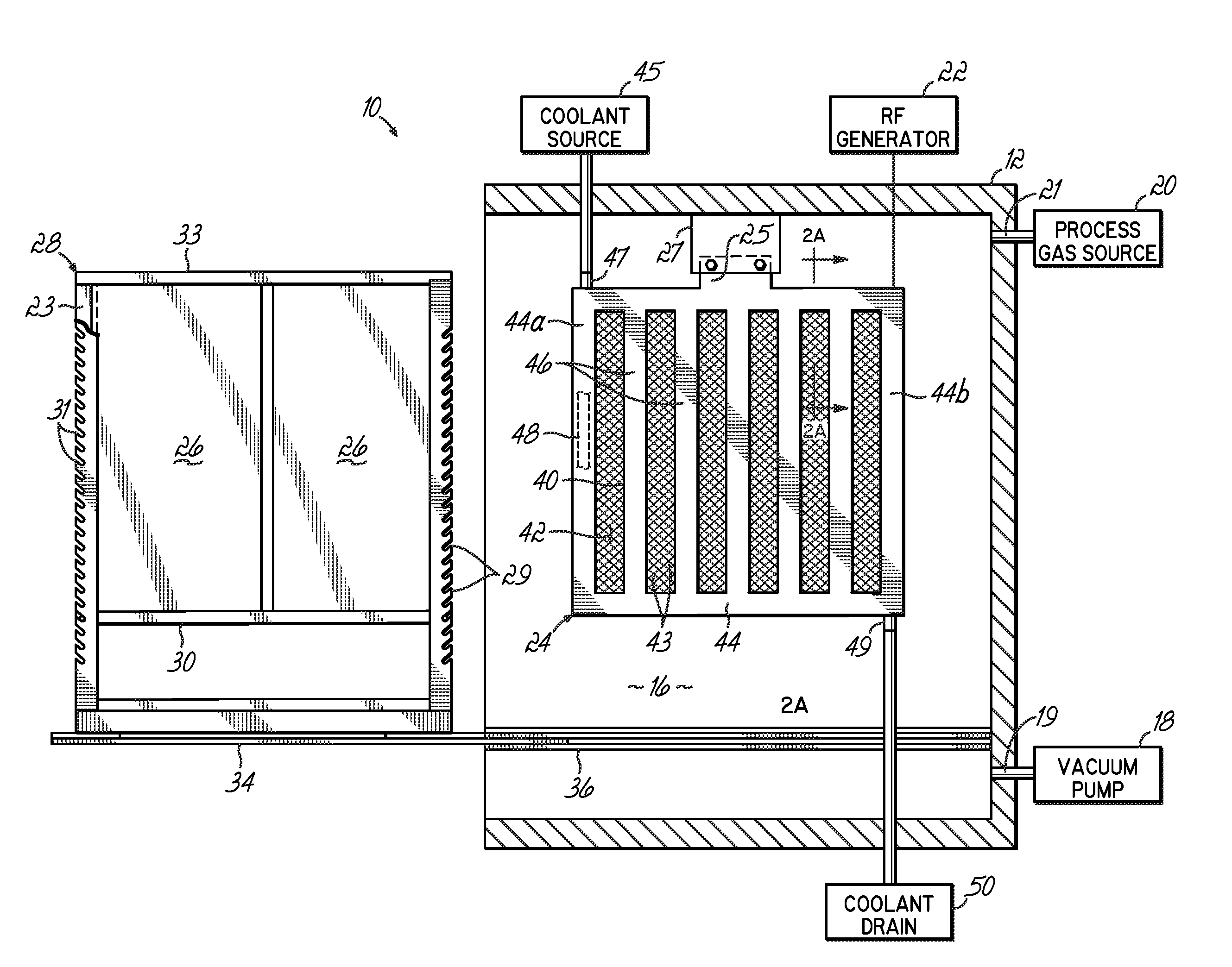
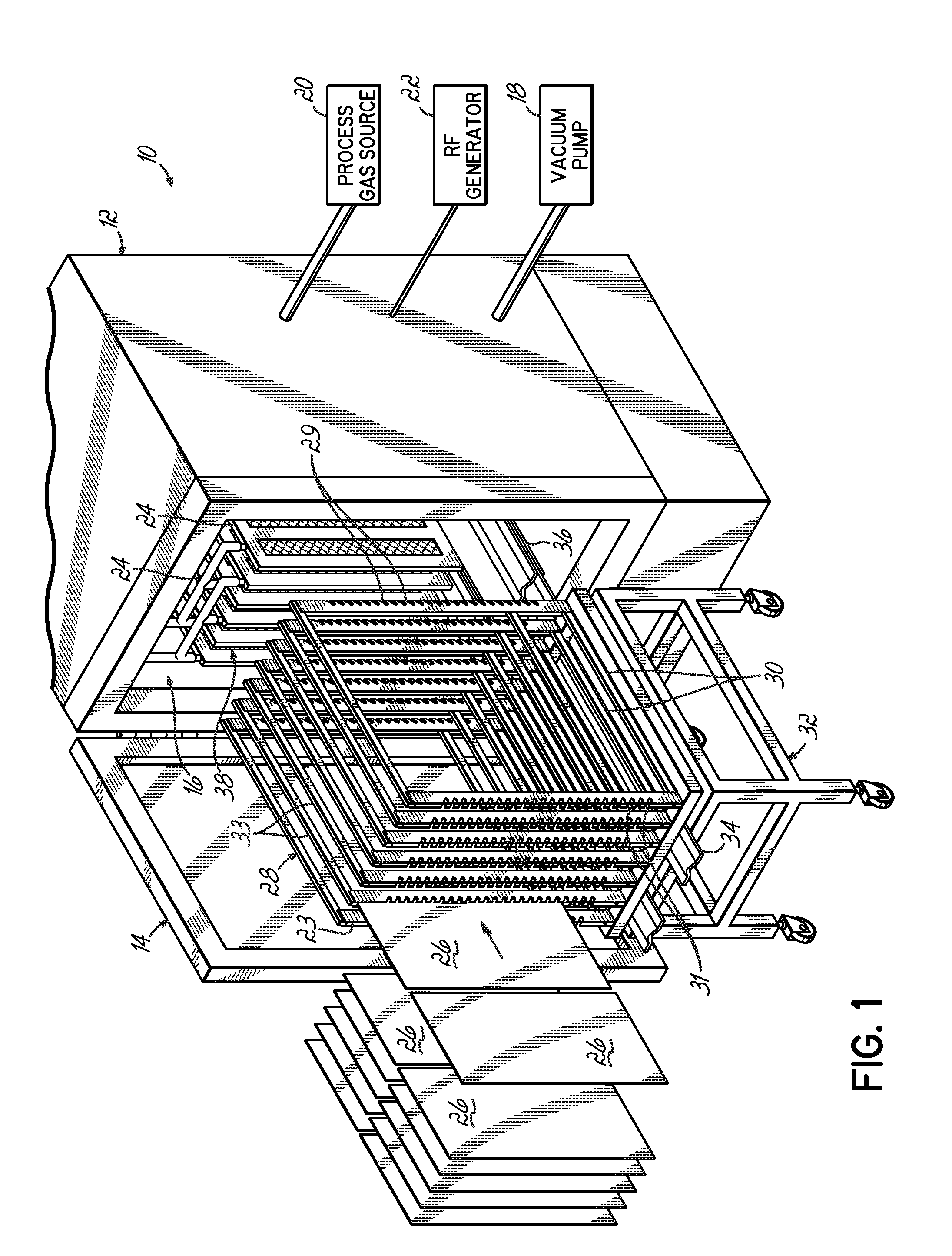
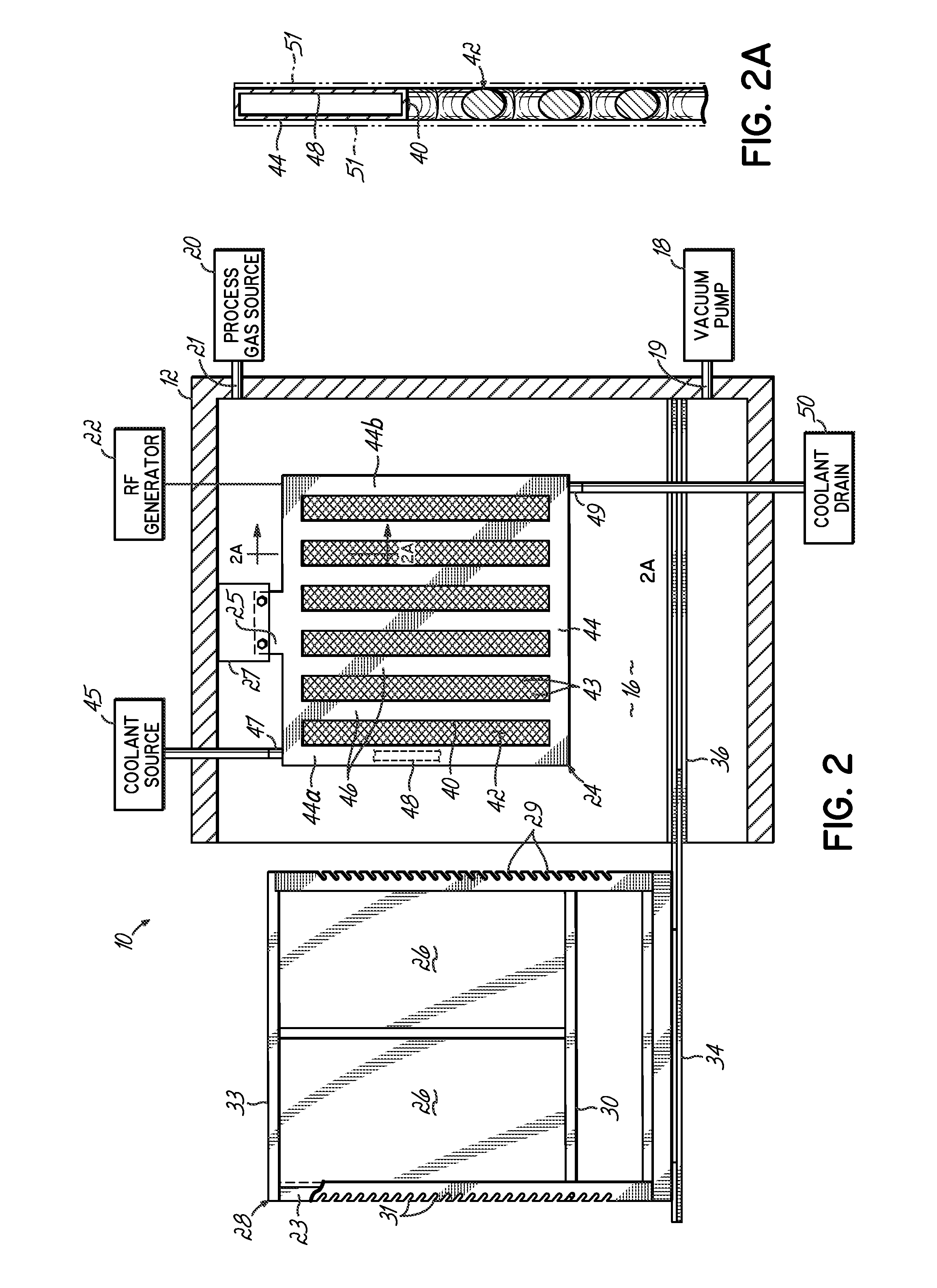
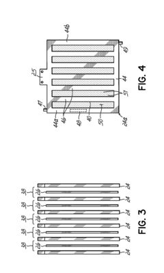
- Plasma treatment equipment and apparatus design: Specialized equipment designs for plasma surface treatment include vacuum chambers, electrode configurations, and gas delivery systems. These apparatuses are engineered to generate stable plasma under controlled conditions, with features such as adjustable power supplies, temperature control mechanisms, and automated process control systems. Advanced designs incorporate multiple treatment zones, rotating substrate holders, and real-time monitoring capabilities to ensure uniform treatment across complex geometries.
- Plasma treatment for semiconductor and electronics applications: In semiconductor manufacturing, plasma treatment is crucial for cleaning, etching, and activating surfaces prior to subsequent processing steps. The technique enables precise modification of electronic components at the nanoscale, improving electrical connections and device performance. Plasma processes are used for removing organic contaminants, oxide layers, and for creating specific surface functionalities that enhance bonding in microelectronic assemblies and integrated circuits.
- Atmospheric pressure plasma treatment methods: Atmospheric pressure plasma treatment eliminates the need for vacuum systems, making it more cost-effective and suitable for continuous processing of large or irregularly shaped objects. This approach uses specialized electrode designs and gas mixtures to generate stable plasma at ambient pressure. The technology enables high-throughput industrial applications including roll-to-roll processing of films, textiles, and other materials, with the ability to selectively treat specific surface areas.
- Plasma surface treatment for polymers and composites: Plasma treatment is particularly effective for modifying polymer and composite surfaces, which are often chemically inert and difficult to bond. The process introduces polar groups, increases surface energy, and creates nanoscale roughness that significantly improves adhesion properties. This enables enhanced bonding of coatings, adhesives, and inks to materials such as polyethylene, polypropylene, and various engineering plastics, while maintaining the bulk mechanical properties of the substrate.
02 Plasma equipment and apparatus design
Various specialized equipment and apparatus designs are used for plasma surface treatment, including vacuum chambers, atmospheric pressure plasma systems, and roll-to-roll processing equipment. These systems incorporate electrodes, power supplies, gas delivery systems, and control mechanisms to generate and maintain stable plasma for consistent surface treatment. Advanced designs focus on energy efficiency, treatment uniformity, and integration with manufacturing lines.Expand Specific Solutions03 Process parameters and optimization for plasma treatment
The effectiveness of plasma surface treatment depends on various process parameters including gas composition, power input, treatment time, pressure, and distance between the plasma source and substrate. Optimization of these parameters is crucial for achieving desired surface properties while minimizing damage to the substrate. Different materials require specific parameter combinations for optimal treatment results.Expand Specific Solutions04 Applications in semiconductor and electronics manufacturing
Plasma surface treatment plays a critical role in semiconductor and electronics manufacturing for cleaning, etching, and activating surfaces prior to deposition or bonding processes. It is used for removing organic contaminants, native oxides, and other impurities from wafer surfaces. The treatment enhances the performance and reliability of electronic components by improving interface properties and reducing defects.Expand Specific Solutions05 Plasma treatment for polymer and composite materials
Plasma treatment is particularly effective for modifying the surface properties of polymers and composite materials. It can introduce functional groups, increase surface energy, and improve adhesion characteristics without altering the bulk properties. This treatment enables better bonding between dissimilar materials, enhances printability, and improves coating adhesion on otherwise low-surface-energy polymers used in packaging, automotive, and aerospace industries.Expand Specific Solutions
Key Industry Players and Competitive Analysis
Plasma surface treatment for electronic components is experiencing rapid growth in a maturing market, with an estimated global value exceeding $2 billion. The technology has reached moderate maturity but continues to evolve with advanced applications. Key industry players represent diverse specializations: semiconductor manufacturing leaders (Applied Materials, Tokyo Electron, TSMC), electronic component specialists (Nordson, Dexerials), and research institutions (CNRS, University of Sydney). The competitive landscape features established corporations with comprehensive solutions alongside specialized firms focusing on niche applications. Recent innovations from companies like LG Electronics and NXP are driving adoption in emerging applications such as flexible electronics and IoT devices, while research collaborations between industry and academia are accelerating technological advancement.
Nordson Corp.
Technical Solution: Nordson has developed advanced plasma surface treatment systems specifically designed for electronic components manufacturing. Their technology utilizes low-pressure plasma chambers that create controlled environments where gases like oxygen, argon, or nitrogen are ionized to form reactive plasma. This plasma interacts with component surfaces at the molecular level, removing organic contaminants and modifying surface properties to enhance adhesion characteristics. Nordson's systems feature precise parameter control for gas flow, power levels, and exposure time, allowing customization for different electronic components. Their plasma treatment solutions are particularly effective for preparing surfaces prior to wire bonding, encapsulation, and conformal coating processes, achieving up to 200% improvement in adhesion strength compared to untreated surfaces.
Strengths: Highly customizable treatment parameters for different electronic components; excellent process control and repeatability; systems designed specifically for electronics manufacturing workflows. Weaknesses: Higher initial capital investment compared to chemical treatments; requires technical expertise for optimal parameter selection; limited effectiveness on certain complex geometries.
Applied Materials, Inc.
Technical Solution: Applied Materials has pioneered plasma surface treatment technology for semiconductor manufacturing with their integrated plasma processing platforms. Their systems employ capacitively coupled plasma (CCP) and inductively coupled plasma (ICP) technologies to deliver precise surface modifications for electronic components. The company's plasma treatment solutions create ultra-clean surfaces by removing organic contaminants at the atomic level while simultaneously activating surfaces to improve wettability and adhesion properties. Applied Materials' plasma systems can process wafers up to 300mm in diameter with nanometer-level precision, utilizing specialized gas chemistries tailored for specific electronic materials including silicon, ceramics, and advanced packaging substrates. Their technology enables critical surface preparation for subsequent processes like thin film deposition, achieving contamination levels below 1010 atoms/cm2 and contact angles reduced by up to 80% for improved wettability.
Strengths: Industry-leading precision and uniformity across large wafer surfaces; seamless integration with semiconductor manufacturing processes; advanced process control systems with real-time monitoring. Weaknesses: Systems primarily optimized for wafer-level processing rather than discrete components; high operational costs including specialized gas requirements; complex setup and maintenance procedures requiring specialized training.
Critical Patents and Technical Innovations
Plasma Treatment System
PatentInactiveUS20100140223A1
Innovation
- A plasma treatment system with a vacuum chamber and a movable chamber lid that allows for varying the vertical dimension to accommodate different workpiece thicknesses, and a plasma excitation source with a grounded plate that filters out ions and electrons, generating a downstream-type plasma with free radicals for chemical action only.
Plasma processing system and plasma treatment process
PatentInactiveUS20060163201A1
Innovation
- A plasma treatment system with a vacuum chamber and perforated electrodes that allow for precise control of plasma density, using RF power to generate plasma and direct gas flow through porous electrodes for uniform treatment of both sides of substrates, including the use of a gas mixture like oxygen and nitrogen trifluoride for specific surface modifications.
Environmental Impact and Sustainability Considerations
Plasma surface treatment for electronic components represents a significant advancement in sustainable manufacturing practices within the electronics industry. When compared to traditional chemical treatment methods, plasma technology demonstrates considerable environmental advantages. Chemical processes typically involve hazardous substances that require careful handling, storage, and disposal protocols, creating substantial environmental risks. In contrast, plasma treatment operates primarily with inert gases like argon, helium, or reactive gases such as oxygen and nitrogen, which pose minimal environmental hazards.
The reduction in chemical waste represents one of the most significant environmental benefits of plasma treatment. Traditional surface preparation methods generate considerable volumes of liquid chemical waste requiring specialized disposal procedures. Plasma processes generate minimal waste streams, with most byproducts being gaseous and easily managed through standard ventilation systems. This dramatic reduction in hazardous waste aligns with increasingly stringent environmental regulations worldwide and helps manufacturers reduce their environmental compliance costs.
Energy efficiency constitutes another critical sustainability advantage of plasma technology. Modern plasma systems are designed to operate with optimized power consumption, particularly when compared to wet chemical processes that often require heating solutions and energy-intensive drying cycles. The cold plasma processes commonly used for electronic components operate at near-ambient temperatures, further reducing energy requirements and associated carbon emissions.
Water conservation represents a particularly valuable sustainability benefit in regions facing water scarcity challenges. Traditional wet chemical processes consume substantial volumes of ultra-pure water for cleaning and rinsing operations. Plasma treatment eliminates this water requirement entirely, operating as a completely dry process. This water conservation aspect has become increasingly important as electronics manufacturing expands in water-stressed regions globally.
From a product lifecycle perspective, plasma-treated components often demonstrate enhanced durability and reliability, potentially extending product lifespans and reducing electronic waste generation. The precise surface modifications achieved through plasma treatment can improve resistance to environmental degradation factors like moisture and oxidation, contributing to longer-lasting electronic devices and components.
As regulatory frameworks increasingly emphasize sustainable manufacturing practices, plasma treatment technologies position manufacturers advantageously for compliance with emerging environmental standards. The technology aligns with circular economy principles by minimizing resource inputs, reducing waste generation, and potentially extending product lifecycles through improved performance characteristics.
Cost-Benefit Analysis of Plasma vs Alternative Treatments
When evaluating plasma surface treatment against alternative methods for electronic components, cost-benefit analysis reveals significant economic advantages despite higher initial equipment investments. Plasma systems typically require capital expenditure ranging from $50,000 to $500,000 depending on scale and capabilities, considerably higher than chemical treatment setups which may cost between $10,000 and $100,000. However, the operational economics present a different picture.
Plasma treatment demonstrates substantially lower recurring costs, with minimal consumable requirements beyond electricity and process gases. Chemical alternatives necessitate ongoing purchases of solvents, acids, or other reagents that accumulate significant expenses over time. Environmental compliance costs further widen this gap, as plasma processes generate minimal waste compared to chemical treatments that require costly disposal protocols and regulatory compliance measures.
The efficiency metrics strongly favor plasma technology. Treatment cycles typically complete in seconds to minutes, whereas chemical processes often require extended immersion times and subsequent drying periods. This time efficiency translates directly to higher throughput capabilities, allowing manufacturers to process more components per hour with less labor involvement.
Quality-related cost factors represent perhaps the most compelling economic argument for plasma adoption. The precision of plasma modification results in significantly lower defect rates compared to alternative treatments. Statistical analysis from industry implementations shows defect reduction of 30-65% when transitioning from chemical to plasma processes, directly impacting yield rates and reducing costly rework or component rejection.
Long-term reliability improvements from plasma-treated components further enhance the value proposition. Components with plasma-modified surfaces demonstrate extended operational lifespans and reduced failure rates in field applications, decreasing warranty claims and replacement costs. These downstream savings, while more difficult to quantify precisely, represent substantial value that compounds over product lifecycles.
Energy consumption analysis reveals that despite plasma's electricity requirements, the total energy footprint often proves lower than alternatives when accounting for the heating, ventilation, and waste treatment energy demands of chemical processes. This translates to both cost savings and alignment with sustainability initiatives that increasingly influence procurement decisions.
When calculating return on investment timeframes, plasma systems typically achieve breakeven within 12-24 months of implementation for medium-volume production environments, with accelerated returns for high-volume applications. This favorable economic profile, combined with the technical advantages, positions plasma treatment as the economically superior choice for electronic component manufacturing despite higher initial capital requirements.
Unlock deeper insights with PatSnap Eureka Quick Research — get a full tech report to explore trends and direct your research. Try now!
Generate Your Research Report Instantly with AI Agent
Supercharge your innovation with PatSnap Eureka AI Agent Platform!