Output buffer circuit with reinforced turning rate

A technology of output buffering and slew rate, applied in improving amplifiers to improve efficiency, instruments, static indicators, etc., can solve the problem that the output buffer circuit cannot effectively provide high driving capability with low power consumption, and general products do not have suitable structures.

CN101800515BInactive Publication Date: 2012-01-04HIMAX TECH LTD +1
0 Cites 0 Cited by

Patent Information

Authority / Receiving Office
CN · China
Patent Type
Patents(China)
Current Assignee / Owner
Publication Date
2012-01-04
Estimated Expiration
Not applicable · inactive patent

Smart Images

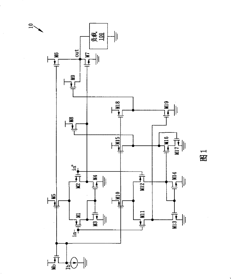
  • Figure 1
    Figure 1
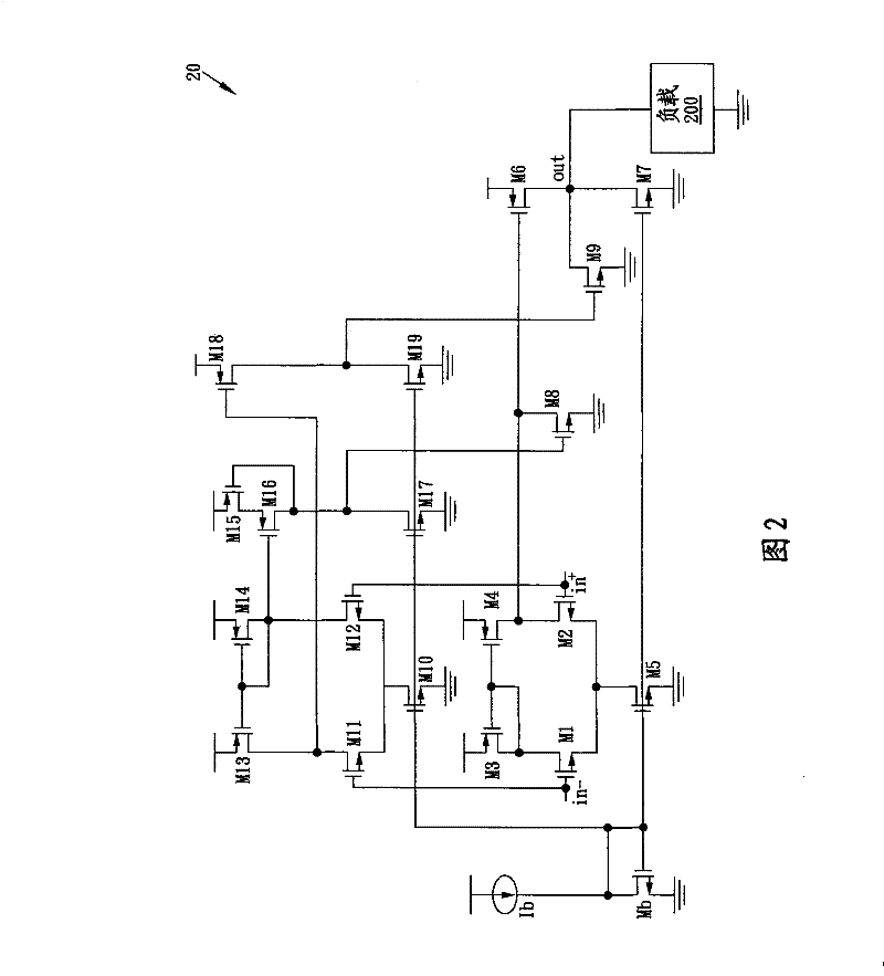
  • Figure 2
    Figure 2
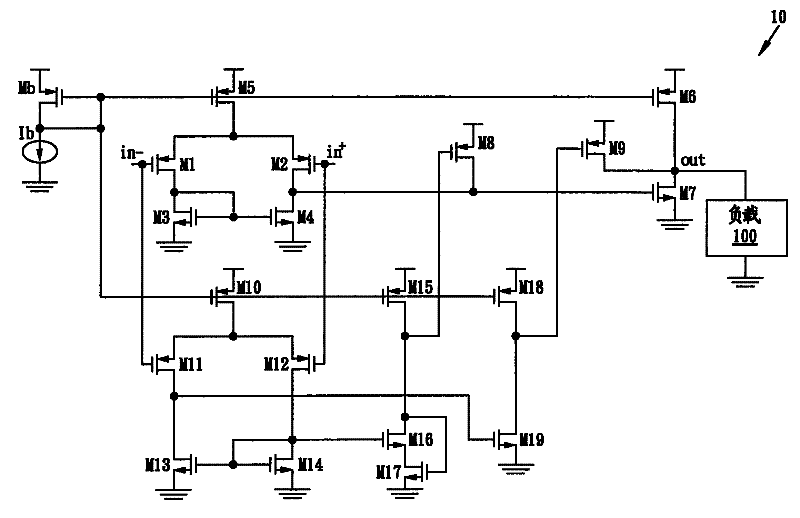
  • Figure 3
    Figure 3
Patent Text Reader

Abstract

The invention relates to an output buffer circuit with a reinforced turning rate. A first turning rate reinforcing transistor and a second turning rate reinforcing transistor are used for reinforcing the turning rates of a source transistor and a drawing transistor of an output level. When the output buffer circuit is in a stable state, a first control circuit and a second control circuit are used for respectively closing the first turning rate reinforcing transistor and the second turning rate reinforcing transistor. When the output buffer circuit is in a rotating state, the first turning rate reinforcing transistor and the second turning rate reinforcing transistor are respectively opened.
Need to check novelty before this filing date? Find Prior Art

Description

technical field

[0001] The invention relates to a buffer amplifier, in particular to a low-power, high-speed output buffer circuit of a display panel source driver. Background technique

[0002] Due to the increasing resolution of flat panel displays (such as liquid crystal displays), thousands of output buffer amplifiers or buffer circuits must be manufactured in the driver integrated circuit. In order to accommodate so many buffer amplifiers in the driver IC, the area of ​​each buffer amplifier must be reduced, and the power consumed by each buffer amplifier, especially the static power consumption, must be reduced. Furthermore, in view of the fact that each row (column) in a large display panel has a relatively large time constant (time constant), in order to provide sufficient driving capability to drive this large panel, it must have a small settling time or a large The slew rate (slewrate). In short, low-power, high-speed output buffer circuits are indispensable for ...

Examples

Embodiment Construction

[0037] In order to further explain the technical means and effects that the present invention adopts to achieve the intended purpose of the invention, below in conjunction with the accompanying drawings and preferred embodiments, the specific implementation, structure, Features and their functions are described in detail below.

[0038] The aforementioned and other technical contents, features and effects of the present invention will be clearly presented in the following detailed description of preferred embodiments with reference to the drawings. Through the description of the specific implementation mode, when the technical means and functions adopted by the present invention to achieve the predetermined purpose can be obtained a deeper and more specific understanding, but the accompanying drawings are only for reference and description, and are not used to explain the present invention be restricted.

[0039] figure 1 A low power, high speed output buffer circuit 10 with...