Pixel circuit

A technology of pixel circuit and conductive layer, applied in the field of pixel circuit, can solve the problem of uneven display image, and achieve the effect of improving image uniformity and reducing offset

Active Publication Date: 2013-07-10
INNOCOM TECH SHENZHEN +1
View PDF5 Cites 12 Cited by
  • Summary
  • Abstract
  • Description
  • Claims
  • Application Information

AI Technical Summary

Problems solved by technology

The threshold voltage (threshold voltage, Vth) of the driving transistor 11 will change with...

Method used


Image

  • Pixel circuit
  • Pixel circuit
  • Pixel circuit

Examples


Embodiment Construction

[0067] In order to make the above objects, features and advantages of the present invention more comprehensible, a preferred embodiment will be described in detail below together with the accompanying drawings.

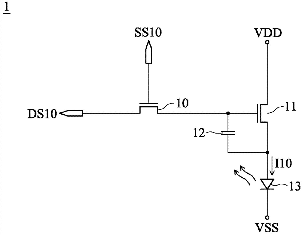
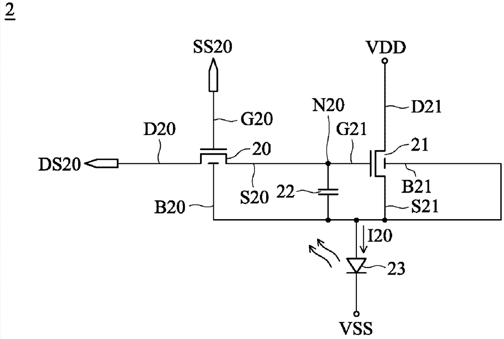
[0068] figure 2 A pixel circuit according to an embodiment of the present invention is shown. refer to figure 2 , the pixel circuit 2 is suitable for an organic light emitting display panel, and includes a switching transistor 20 , a driving transistor 21 , a capacitor 22 , and a diode 23 . In this embodiment, both the switching transistor 20 and the driving transistor 21 are implemented as a double-gate transistor. Such as figure 2 As shown, the switching transistor 20 has an upper gate terminal B20, a lower gate terminal G20, and two electrode terminals D20 and S20. In this embodiment, the two terminals D20 and S20 of the switch transistor 20 are respectively a drain terminal and a source terminal. The driving transistor 21 has an upper gate terminal B21, a ...


PUM


Abstract

The invention discloses a pixel circuit. The pixel circuit comprises a switch transistor, a driving transistor and a first diode. The switch transistor is provided with a first grid end receiving a scanning signal, a first electrode end receiving a data signal and a second electrode end. The driving transistor is provided with a first grid end electrically connected to a second electrode end of the switch transistor, a second grid end, a first electrode end electrically connected with a first voltage source and a second electrode end, the second grid end of the driving transistor is electrically connected with a second voltage source through the first diode, and the voltage supplied by the second voltage source is lower than the voltage supplied by the first voltage source. The pixel circuit can reduce offset of critical voltage, thereby promoting uniformity of images.

Description

technical field [0001] The present invention relates to a pixel circuit, in particular to a pixel circuit using double-gate transistors to improve image uniformity. Background technique [0002] figure 1 Represents a pixel circuit of an existing organic light-emitting display. refer to figure 1 , the pixel circuit 1 includes a switching transistor 10 , a driving transistor 11 , a capacitor 12 , and a light emitting diode 13 . The switch transistor 10 is controlled by a scan signal SS10 and receives a data signal DS10. When the switch transistor 10 is turned on according to the scan signal SS10 , the driving transistor 11 generates a driving current I10 according to the data signal DS10 to drive the LED 13 to emit light. The threshold voltage (threshold voltage, Vth) of the driving transistor 11 will change with the operation time, which will cause the phenomenon of image non-uniformity (mura) on the display. Contents of the invention [0003] The invention provides a ...

Claims


Application Information

Patent Timeline
IPC IPC(8): G09G3/32G09G3/3208
Inventor 周政旭郭鸿儒林信宏
Owner INNOCOM TECH SHENZHEN
Why Eureka
Try Eureka