Array substrate, display panel and display device

An array substrate and display area technology, applied in static indicators, instruments, nonlinear optics, etc., can solve the problems of inaccurate grayscale display of images, affecting transmittance, and changing the deflection angle of liquid crystal molecules, so as to improve the display effect. Effect

Active Publication Date: 2015-09-09
BOE TECH GRP CO LTD +1
View PDF5 Cites 0 Cited by
  • Summary
  • Abstract
  • Description
  • Claims
  • Application Information

AI Technical Summary

Problems solved by technology

[0007] at the gate turn-on voltage from V gh changes to the shutdown voltage V gl At the moment, due to the sudden change of the voltage on the gate, the parasitic capacitance C gd The internal charge moves, and once the charge moves it will cause C gd The voltage at both ends changes, and this voltage change will be conducted from the drain to the pixel electrode 104, causing the electric field strength between the color filter substrate and the array substrate to change, and the electric field strength between the color filter substrate and the array substrate to change It will also cause the deflection angle of the liquid crystal molecules to change, thereby affecting the transmittance, resulting in inaccurate grayscale display of the image

Method used


Image

  • Array substrate, display panel and display device
  • Array substrate, display panel and display device
  • Array substrate, display panel and display device

Examples


Embodiment Construction

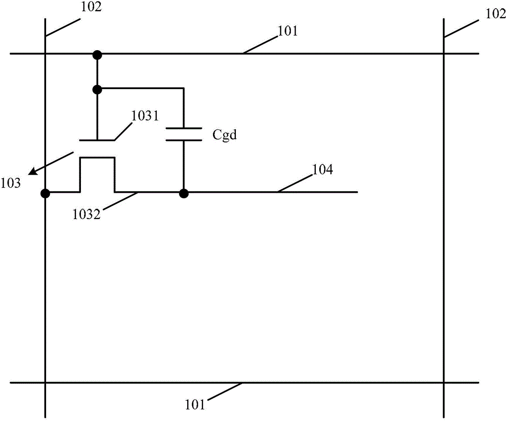
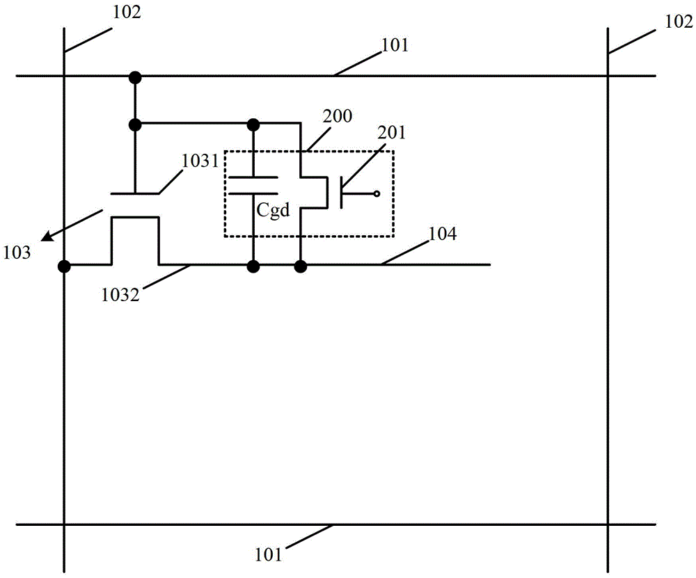
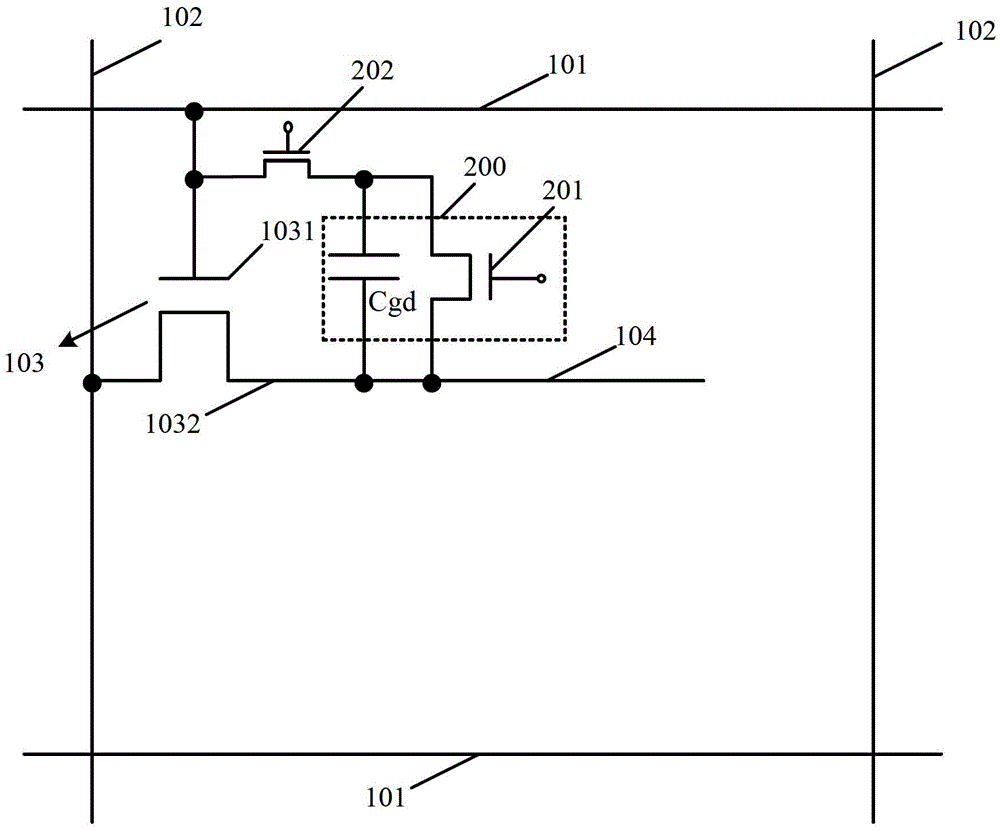
[0034] In the array substrate, display panel, and display device of the embodiments of the present invention, a switch circuit is provided to turn on both ends of the parasitic capacitance when the gate driving signal of the TFT transitions from a high level to a low level. The phenomenon of charge movement does not occur inside the parasitic capacitance, therefore, the influence of the parasitic capacitance between the gate and the drain on the voltage of the pixel electrode is reduced, and the display effect is improved.

[0035] The array substrate of the embodiment of the present invention includes:

[0036] Dividing the display area into a plurality of data lines and a plurality of gate lines in a plurality of sub-display areas;

[0037] a pixel electrode disposed in each sub-display area; and

[0038] A TFT arranged in each sub-display area, the source is electrically connected to the data line, the drain is electrically connected to the pixel electrode, and the gate is...


PUM


Abstract

The present disclosure provides an array substrate, a display panel and a display device. The array substrate includes: a plurality of data lines and a plurality of gate lines configured to divide a display region into a plurality of display sub-regions; a pixel electrode arranged at each display sub-region; and a TFT arranged at each display sub-region, a source electrode of the TFT being electrically connected to the data line, a drain electrode thereof being electrically connected to the pixel electrode and a gate electrode thereof being electrically connected to the gate line, wherein a parasitic capacitor is formed between the gate electrode and the drain electrode of the TFT. The array substrate further includes a switch circuit configured to enable both ends of the parasitic capacitor to be electrically connected when a gate driving signal of the TFT is changed from a high level to a low level.

Description

technical field [0001] The present invention relates to the field of display technology, in particular to an array substrate, a display panel and a display device. Background technique [0002] The display device based on liquid crystal is a kind of flat display widely used at present. Compared with other display methods, it has the advantages of low power consumption, light weight, and no radiation. [0003] A liquid crystal-based display device generally includes an array substrate, a color filter substrate, and a liquid crystal layer. Such as figure 1 As shown, the display area on the array substrate includes multiple sub-display areas, and each sub-display area is generally formed by crossing and surrounding two gate lines 101 (scanning lines) and two data lines 102 . [0004] Such as figure 1 As shown, a thin film transistor 103 and a pixel electrode 104 are disposed inside the sub-display region. By controlling the voltage applied to the common electrode and / or the...

Claims


Application Information

Patent Timeline
Patent Type & Authority Patents(China)
IPC IPC(8): G02F1/1368
CPCG02F1/13624G02F2001/13606G02F1/13606G09G3/3607G09G3/3655G09G2300/0819G09G2300/0876G09G2320/0233
Inventor 王洁琼
Owner BOE TECH GRP CO LTD
Why Eureka
Try Eureka