Current blocking layer and light emitting diode chip manufacturing method

A technology of current blocking layer and manufacturing method, which is applied in the direction of circuits, electrical components, semiconductor devices, etc., and can solve the problems of high voltage and low antistatic ability of light-emitting diode chips

Active Publication Date: 2017-09-22
HC SEMITEK ZHEJIANG CO LTD
View PDF3 Cites 4 Cited by
  • Summary
  • Abstract
  • Description
  • Claims
  • Application Information

AI Technical Summary

Problems solved by technology

[0006] In order to solve the problems of high voltage and low antistatic ability of light-emitting diode chips in the prior art, an embodiment of the present invention provides a method for manufacturing a current blocking layer and a light-emitting diode chip

Method used


Image

  • Current blocking layer and light emitting diode chip manufacturing method
  • Current blocking layer and light emitting diode chip manufacturing method
  • Current blocking layer and light emitting diode chip manufacturing method

Examples


Embodiment 1

[0042] The embodiment of the present invention provides a method for fabricating a current blocking layer, see figure 1 , the production method includes:

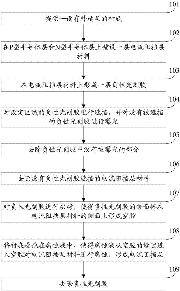
[0043] Step 101: Provide a substrate with an epitaxial layer.

[0044] Figure 2a It is a schematic diagram of a partial structure of the LED chip after step 101 is executed. Among them, 10 is the substrate with the epitaxial layer.

[0045] In this embodiment, the epitaxial layer includes an N-type semiconductor layer, a light-emitting layer, and a P-type semiconductor layer stacked on the substrate in sequence. grooves in the semiconductor layer.

[0046] Specifically, the substrate may be a sapphire substrate or a silicon substrate. The N-type semiconductor layer may be an N-type GaN layer, and the P-type semiconductor layer may be a P-type GaN layer. The light-emitting layer may include multiple InGaN layers and multiple GaN layers, and the multiple InGaN layers and multiple GaN layers are alternately stacked.

...

Embodiment 2

[0098] An embodiment of the present invention provides a method for manufacturing a current blocking layer, which is a specific implementation of the method provided in Embodiment 1, see image 3 , the production method includes:

[0099] Step 201: Provide a substrate with an epitaxial layer.

[0100] Step 202: Deposit a layer of current blocking layer material with a thickness of 2000 angstroms on the P-type semiconductor layer and the N-type semiconductor layer.

[0101] Step 203: Coating an adhesion promoter on the material of the current blocking layer.

[0102] Step 204: Coating a negative photoresist with a thickness of 2 microns on the tackifier.

[0103] Step 205: Exposing the negative photoresist on the current blocking layer with an exposure energy of 90mj / cm 2 .

[0104] Step 206: Use a developer solution with a concentration of 2.38% to remove the part of the negative photoresist that has not been exposed, and the angle formed between the side and the bottom of...

Embodiment 3

[0111] An embodiment of the present invention provides a method for manufacturing a light emitting diode chip, see Figure 4 , the production method includes:

[0112] Step 301: Provide a substrate with an epitaxial layer.

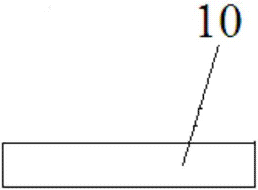
[0113] Figure 5a It is a schematic structural diagram of the LED chip after step 301 is executed. Wherein, 10 is a substrate provided with an epitaxial layer.


PUM


Abstract

The invention discloses a current blocking layer and a light emitting diode chip manufacturing method, which belongs to the technical field of semiconductors. The method comprises the steps that a substrate provided with an epitaxial layer is provided; a current blocking layer material is laid on a P-type semiconductor layer and an N-type semiconductor layer; a negative photoresist is formed on the current blocking layer material; the negative photoresist in a set region is blocked, and the negative photoresist which is not blocked is exposed; a part which is not exposed in the negative photoresist is removed; the current blocking layer material without the negative photoresist barrier is removed; the negative photoresist is baked, so that the side of the negative photoresist is taken on the side of the current blocking layer material to form a cavity; the substrate is immersed in an etching solution, so that the etching solution enters the cavity from the cavity gap to corrode the current blocking layer material to form a current blocking layer; the angle between the side and the bottom of the current blocking layer is corroded into an acute angle; and the negative photoresist is removed. According to the invention, the voltage can be reduced, and the antistatic ability is improved.

Description

technical field [0001] The invention relates to the technical field of semiconductors, in particular to a method for manufacturing a current blocking layer and a light emitting diode chip. Background technique [0002] Light Emitting Diode (English: Light Emitting Diode, referred to as: LED) is a semiconductor electronic device that converts electrical energy into light energy. Gallium nitride (GaN)-based light-emitting diodes are widely used light-emitting diodes, which have the advantages of low voltage, low power consumption, small size, light weight, long life and high reliability. [0003] The chip is the most important component of the LED. Existing light-emitting diode chips usually include a substrate and an N-type semiconductor layer, a light-emitting layer, and a P-type semiconductor layer stacked on the substrate in sequence. To the groove of the N-type semiconductor layer, the P-type semiconductor layer is provided with a current blocking layer, and the cross s...

Claims


Application Information

Patent Timeline
Patent Type & Authority Applications(China)
IPC IPC(8): H01L33/14H01L33/20
CPCH01L33/145H01L33/20
Inventor 兰叶顾小云徐瑾吴志浩杨春艳王江波
Owner HC SEMITEK ZHEJIANG CO LTD
Why Eureka
Try Eureka