Method for preparing pyramid array on monocrystalline silicon substrate

A single-crystal silicon and single-crystal silicon wafer technology, which is applied in the field of preparing pyramid arrays, can solve the problems of difficulty in preparing nanoscale photolithography masks, complicated processes, limited applications, etc., and achieves excellent light trapping effect, simple operation, top-end smooth effect

Active Publication Date: 2013-05-22
HUANGSHAN AKENT SEMICON TECH
View PDF5 Cites 33 Cited by
  • Summary
  • Abstract
  • Description
  • Claims
  • Application Information

AI Technical Summary

Problems solved by technology

This method is not only complicated in process and relatively high in cost, but it is still difficult to prepare a photolithography mask at the nanoscale, which limits its application in large-scale industrialization and in the preparation of nanoscale small-scale pyramid arrays.

Method used


Image

  • Method for preparing pyramid array on monocrystalline silicon substrate
  • Method for preparing pyramid array on monocrystalline silicon substrate
  • Method for preparing pyramid array on monocrystalline silicon substrate

Examples


Embodiment 1

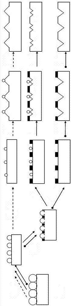
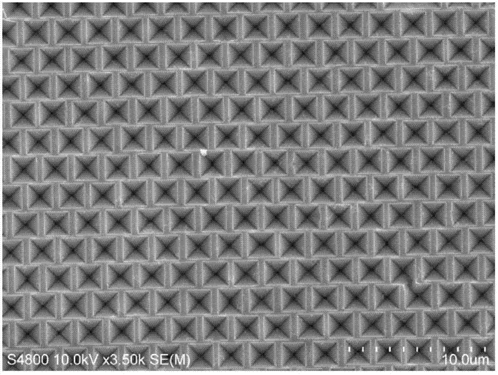
[0065] Preparing a positive pyramid array on a single crystal silicon substrate comprises the following steps:

[0066] (1) Arrange a layer of hexagonal close-packed polystyrene colloidal microspheres on the monocrystalline silicon wafer substrate by the vertical pulling method, and the pulling speed is 1 μm / s. The sheet was dried naturally in the air for 1 hour, and then subjected to rapid thermal annealing, the annealing temperature was 115°C, the glass transition temperature of polystyrene microspheres was 120°C, and the annealing time was 2 minutes and 30 seconds;

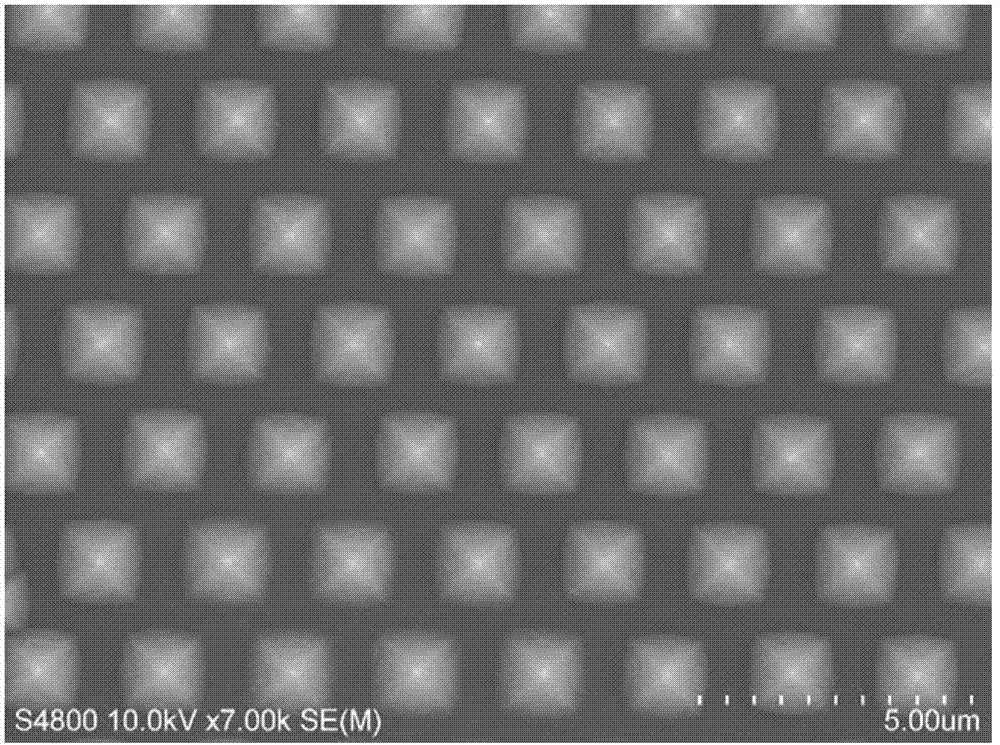
[0067](2) Using the inductively coupled plasma etching method, the microspheres are etched in an atmosphere of oxygen, so that the microspheres closely packed on the surface of the single crystal silicon wafer are separated from each other, and the diameter of the etched microspheres is determined by the The etching parameters and etching time are determined, the etching power is 150 watts, and the etching time...

Embodiment 2

[0072] Preparing a positive pyramid array on a single crystal silicon substrate comprises the following steps:

[0073] (1) Arrange a layer of hexagonal close-packed polystyrene colloidal microspheres on the monocrystalline silicon wafer substrate by vertical pulling method at a pulling speed of 2.5 μm / s. The sheet was dried naturally in the air for 1 hour, and then subjected to rapid thermal annealing, the annealing temperature was 125°C, the glass transition temperature of polystyrene microspheres was 120°C, and the annealing time was 1 minute and 30 seconds;

[0074] (2) Using the inductively coupled plasma etching method, the microspheres are etched in an atmosphere of oxygen, so that the microspheres closely packed on the surface of the single crystal silicon wafer are separated from each other, and the diameter of the etched microspheres is determined by the The etching parameters and etching time are determined, the etching power is 200 watts, and the etching time is 1 ...

Embodiment 3

[0079] Prepare an array of inverted pyramids on a single crystal silicon substrate, comprising the following steps:

[0080] (1) Arrange a layer of hexagonal close-packed polystyrene colloidal microspheres on the monocrystalline silicon wafer substrate by vertical pulling method at a pulling speed of 1.3 μm / s. The sheet was dried naturally in the air for 1 hour, and then subjected to rapid thermal annealing, the annealing temperature was 115°C, the glass transition temperature of polystyrene microspheres was 120°C, and the annealing time was 2 minutes;

[0081] (2) Using the inductively coupled plasma etching method, the microspheres are etched in an atmosphere of oxygen, so that the microspheres closely packed on the surface of the single crystal silicon wafer are separated from each other, and the diameter of the etched microspheres is determined by the The etching parameters and etching time are determined, the etching power is 125 watts, and the etching time is 3 minutes; ...


PUM

PropertyMeasurementUnit
thicknessaaaaaaaaaa

Abstract

The invention relates to a method for preparing a pyramid array on a monocrystalline silicon substrate, and belongs to the technical field of manufacture of photovoltaic and semiconductor devices. The method comprises the following steps of: covering microballons in periodic arrangement on the surface of a monocrystalline silicon piece, and annealing near the glass transition temperature point of the microballoon; in oxygen atmosphere, obtaining a microballoon array in separation arrangement after etching by use of inductive coupling plasma; depositing a metallic titanium membrane on the monocrystalline silicon piece uniformly by a physical vapor deposition manner; and putting a silicon wafer with a masking film into an alkaline solution containing a surfactant for corrosion so as to obtain the pyramid array in order arrangement. The method is simple in process, short in preparation period and mature in technology; and three structures such as a positive pyramid array, an inverted pyramid array and a positive and inverted pyramid combined array can be obtained by a method for preparing a template through selecting and fine turning. The method has wide application value in the fields of photovoltaic, magnetic memory devices, nano photoelectric devices, nano sensors, surface raman enhancement and surface plasma effect and the like.

Description

technical field [0001] The invention relates to a method for preparing a pyramid array on a single crystal silicon substrate, belonging to the technical field of photovoltaic and semiconductor device manufacturing. Background technique [0002] Pyramid arrays with uniform size and orderly arrangement period not only have special size and shape effects, but also have good optical, electrical and magnetic properties. The photovoltaic industry often uses the alkaline texture method to prepare randomly distributed positive pyramid light-trapping surfaces to increase light absorption and thus improve battery conversion efficiency. However, regular alkaline texture methods usually produce positive pyramids, and the pyramids do not have periodicity and uniformity at all. At present, among the monocrystalline silicon cells, the PERL cell with the highest efficiency (25%) uses a regular inverted pyramid array prepared by photolithography technology as the surface anti-reflective str...

Claims


Application Information

Patent Timeline
Patent Type & Authority Applications(China)
IPC IPC(8): B81C1/00
Inventor 董刚强刘丰珍
Owner HUANGSHAN AKENT SEMICON TECH
Why Eureka
Try Eureka