Array substrate and display device

A technology for array substrates and substrate substrates, applied in the fields of instruments, nonlinear optics, optics, etc., can solve the problems of reducing the delay of public voltage signals and flickering phenomena of display devices, and achieve the goals of reducing delays, improving flickering phenomena, and improving display effects Effect

Active Publication Date: 2013-10-16
BEIJING BOE OPTOELECTRONCIS TECH CO LTD
View PDF5 Cites 22 Cited by
  • Summary
  • Abstract
  • Description
  • Claims
  • Application Information

AI Technical Summary

Problems solved by technology

[0005] The present invention provides an array substrate, which is used to improve the problem of flickering when the display device is in use, and at the same time reduce the delay in the transmission process of the common voltage signal, so as to prevent the occurrence of bad crosstalk

Method used


Image

  • Array substrate and display device
  • Array substrate and display device
  • Array substrate and display device

Examples


Embodiment Construction

[0034] The following will clearly and completely describe the technical solutions in the embodiments of the present invention with reference to the accompanying drawings in the embodiments of the present invention. Obviously, the described embodiments are only some, not all, embodiments of the present invention. Based on the embodiments of the present invention, all other embodiments obtained by persons of ordinary skill in the art without making creative efforts belong to the protection scope of the present invention.

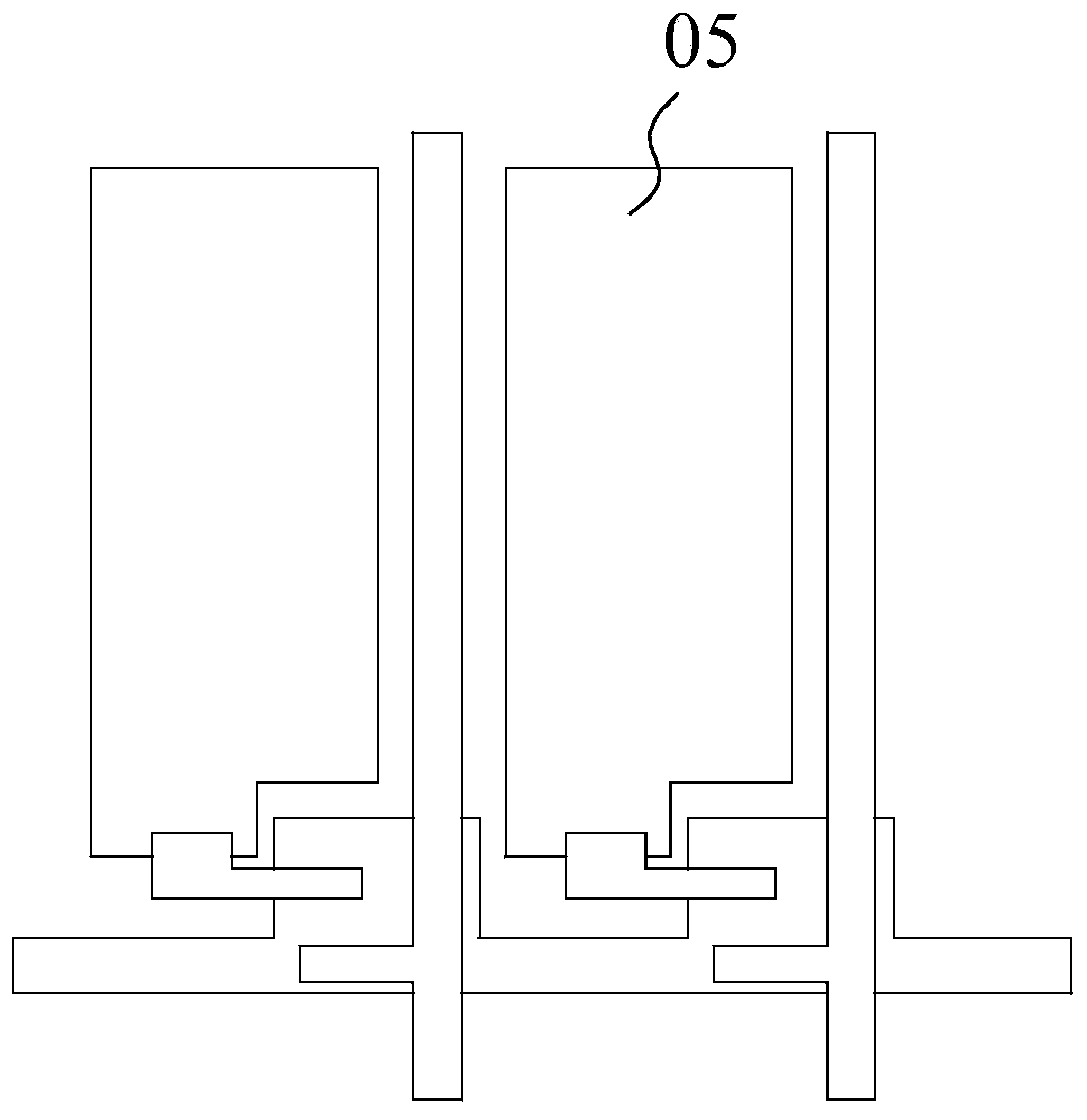
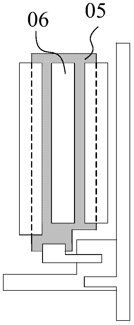
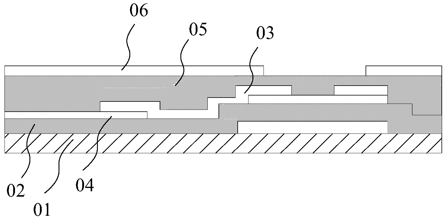
[0035] Please refer to Figure 4 , Figure 5 The present invention provides an array substrate, including a common electrode line 8, and a plurality of pixel units distributed in an array, and each pixel unit includes a first common electrode 2, a pixel electrode 3, And the second common electrode 4, the pixel electrode 3 is a plate electrode, and the second common electrode 4 is a slit electrode; an insulating protective layer 5 is provided between the pixel...


PUM


Abstract

The invention discloses an array substrate and a display device. The array substrate comprises a public electrode wire and a plurality of pixel units distributed in an array manner, wherein each pixel unit comprises a first public electrode, a pixel electrode and a second public electrode which are located on a substrate and arranged sequentially, wherein the pixel electrode adopts a plate electrode, and the second public electrode adopts a slit electrode; an insulation protective layer is arranged between the pixel electrode and the second public electrode, and between the pixel electrode and the first public electrode respectively, and projections of the pixel electrode, the first public electrode and the second public electrode on the substrate are overlapped; and the first public electrode and the second public electrode are electrically connected with the public electrode wire. The array substrate effectively solves the problem of a blinking phenomenon of the display device during use and reduces delay during the transmission process of a public voltage signal simultaneously, so that harmful crosstalk is prevented, and the display effect of the display device is improved.

Description

technical field [0001] The invention relates to the technical field of liquid crystal display, in particular to an array substrate and a display device. Background technique [0002] In the field of liquid crystal display technology, the Advanced Super Dimension Switch (ADS) type array substrate has the advantages of wide viewing angle, etc., so it is widely used. ADS technology mainly forms a multi-dimensional electric field through the electric field generated by the edge of the slit electrode in the same plane and the electric field generated between the slit electrode layer and the plate electrode layer, so that all aligned liquid crystal molecules between the slit electrodes and directly above the electrodes in the liquid crystal cell Both can generate rotation, thereby improving the working efficiency of the liquid crystal and increasing the light transmission efficiency. Advanced ultra-dimensional field conversion technology can improve the picture quality of TFT-LCD...

Claims


Application Information

Patent Timeline
Patent Type & Authority Applications(China)
IPC IPC(8): G02F1/1343
CPCG02F1/134309G02F2201/121G02F1/134318G02F1/134363G02F1/133345G02F1/134336G02F1/13439
Inventor 姜文博
Owner BEIJING BOE OPTOELECTRONCIS TECH CO LTD
Why Eureka
Try Eureka