Test pad sharing circuit

A circuit and test control technology, applied in the direction of electronic circuit testing, etc., can solve the problems of wasting chip area and low efficiency, and achieve the effect of reducing the number and reducing the waste of chip area

Active Publication Date: 2014-04-30
SHANGHAI HUAHONG GRACE SEMICON MFG CORP
View PDF6 Cites 0 Cited by
  • Summary
  • Abstract
  • Description
  • Claims
  • Application Information

AI Technical Summary

Problems solved by technology

Although this structure allows one test pad to test two circuits, it is still not efficient and wastes chip area

Method used


Image

  • Test pad sharing circuit
  • Test pad sharing circuit

Examples


Embodiment Construction

[0016] The implementation of the present invention is described below through specific examples and in conjunction with the accompanying drawings, and those skilled in the art can easily understand other advantages and effects of the present invention from the content disclosed in this specification. The present invention can also be implemented or applied through other different specific examples, and various modifications and changes can be made to the details in this specification based on different viewpoints and applications without departing from the spirit of the present invention.

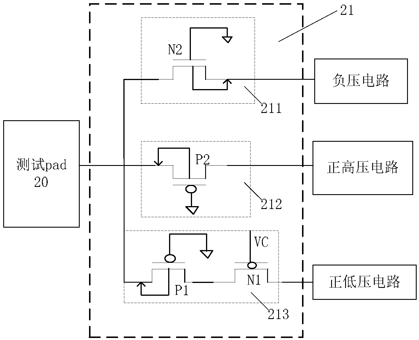
[0017] figure 2 It is a circuit diagram of a preferred embodiment of a test pad sharing circuit of the present invention. Such as figure 2 As shown, a test pad sharing circuit of the present invention enables a negative voltage circuit, a positive high voltage circuit and a positive low voltage circuit to share one test pad, which includes: a test pad 20 and a control circuit 21 .

[00...


PUM


Abstract

The invention discloses a test pad sharing circuit. The circuit comprises a test pad and a control circuit. The control circuit is used for connecting the test pad, a negative-voltage circuit, a positive high-voltage circuit and a positive low-voltage circuit so as to control the test pad to carry out input or output testing on the negative-voltage circuit, the positive high-voltage circuit and the positive low-voltage circuit respectively according to the testing purposes. A small number of MOS tubes are added, the area is not increased much, but the number of testing pads is effectively reduced, and accordingly the area waste of a chip is effectively reduced.

Description

technical field [0001] The present invention relates to a test pad sharing circuit, in particular to a test pad sharing circuit that enables the test pad to test multiple circuits. Background technique [0002] At present, integrated circuits are becoming more and more complex, their functions are becoming more and more powerful, and the manufacturing process is becoming more and more advanced. The typical process line width is only 0.18um, 0.13um, 90nm, 45nm or even narrower. In order to ensure the normal operation of each circuit, In addition to testing on the normal pins outside the bare chip (Die), some test pads are usually placed at some key points to facilitate problem tracking when problems occur. As the complexity of integrated circuits increases, more and more points need to be placed on the tracking pads, because the test pads generally have a large area such as 60×60um, and it is generally not suitable to place circuits on the top and bottom, so placing more test...

Claims


Application Information

Patent Timeline
Patent Type & Authority Applications(China)
IPC IPC(8): G01R31/28
Inventor 杨光军
Owner SHANGHAI HUAHONG GRACE SEMICON MFG CORP
Why Eureka
Try Eureka