

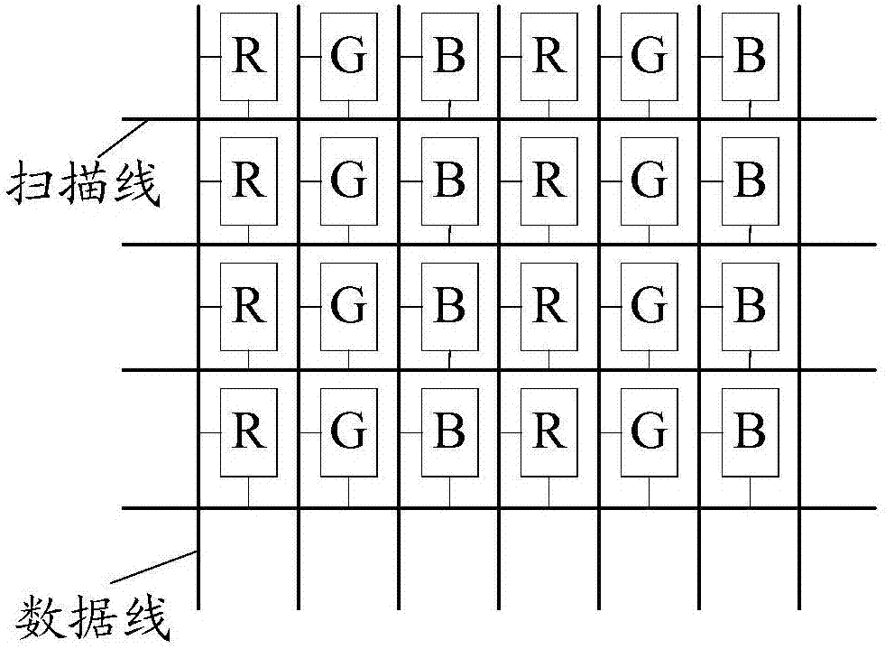
Pixel structure and array substrate
A pixel structure and pixel electrode technology, applied in nonlinear optics, instruments, optics, etc., can solve the problems of reducing the transmittance of liquid crystal panels, loss of pixel aperture ratio, etc.
- Summary
- Abstract
- Description
- Claims
- Application Information
AI Technical Summary
Problems solved by technology
Method used
Image

Examples
Embodiment Construction
[0024] The following will clearly and completely describe the technical solutions in the embodiments of the present invention with reference to the drawings in the embodiments of the present invention. Apparently, the described embodiments are some, not all, embodiments of the present invention. Based on the implementation manners in the present invention, all other implementation manners obtained by persons of ordinary skill in the art without making creative efforts shall fall within the protection scope of the present invention.
[0025] In addition, the following descriptions of the various embodiments refer to the attached drawings to illustrate specific embodiments in which the present invention can be implemented. The directional terms mentioned in the present invention, for example, "upper", "lower", "front", "rear", "left", "right", "inner", "outer", "side", etc., only is to refer to the direction of the attached drawings. Therefore, the direction terms used are for ...
PUM
 Abstract
Description
Claims
Application Information