

PCB stitching clamp device
A fixture device and matching block technology, which is applied in the direction of laminated printed circuit boards, assembled printed circuits with electrical components, electrical components, etc., can solve the problems of different positions of pressing areas, increase material costs and production costs, and achieve smart design , material saving, and convenient operation
- Summary
- Abstract
- Description
- Claims
- Application Information
AI Technical Summary
Problems solved by technology
Method used
Image

Examples
Embodiment Construction
[0019] The implementation structure of the present invention will be described below in conjunction with the accompanying drawings.
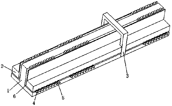
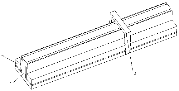
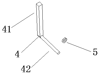
[0020] like Figure 1 to Figure 5 As shown, the fixture device for pressing PCB of the present invention includes a main body block 1, a mating block 2, a fixed block 3, an L-shaped support 4 and a nut 5; the main body block 1 is T-shaped, and the mating block 2 is set There are two pieces, symmetrically arranged on both sides of the main block 1; the main block 1 and the matching block 2 are connected and fixed by the fixing block 3, and an L-shaped sliding channel 6 is formed between the main block 1 and the matching block 2; the sliding channel 6 can accommodate a plurality of L-shaped supports 4, the vertical length and horizontal length of the L-shaped support 4 are respectively greater than the vertical length and the horizontal length of the sliding channel 6; the L-shaped support 4 is composed of a cuboid 41 and The other end is integra...
PUM
 Abstract
Description
Claims
Application Information