Display panel, manufacturing method of display panel and display device

A display panel and manufacturing method technology, which is applied in semiconductor/solid-state device manufacturing, organic semiconductor devices, semiconductor devices, etc., can solve the problems of display panel damage, uneven force on the display motherboard, etc., to avoid uneven force, Guarantee the effect of appearance and quality

Pending Publication Date: 2018-06-29
BOE TECH GRP CO LTD +1
View PDF0 Cites 14 Cited by
  • Summary
  • Abstract
  • Description
  • Claims
  • Application Information

AI Technical Summary

Problems solved by technology

[0004] The present invention provides a display panel, its manufacturing method, and a display device, which can solve the problem of uneven force on the display mother board in the cutting process due to the fact that the glass glue may not completely cover the cutting line area in the related art, and the display obtained after cutting. The problem that the panel may be damaged, the technical solution is as follows:

Method used


Image

  • Display panel, manufacturing method of display panel and display device
  • Display panel, manufacturing method of display panel and display device
  • Display panel, manufacturing method of display panel and display device

Examples


Embodiment Construction

[0054] In order to make the object, technical solution and advantages of the present invention clearer, the implementation manner of the present invention will be further described in detail below in conjunction with the accompanying drawings.

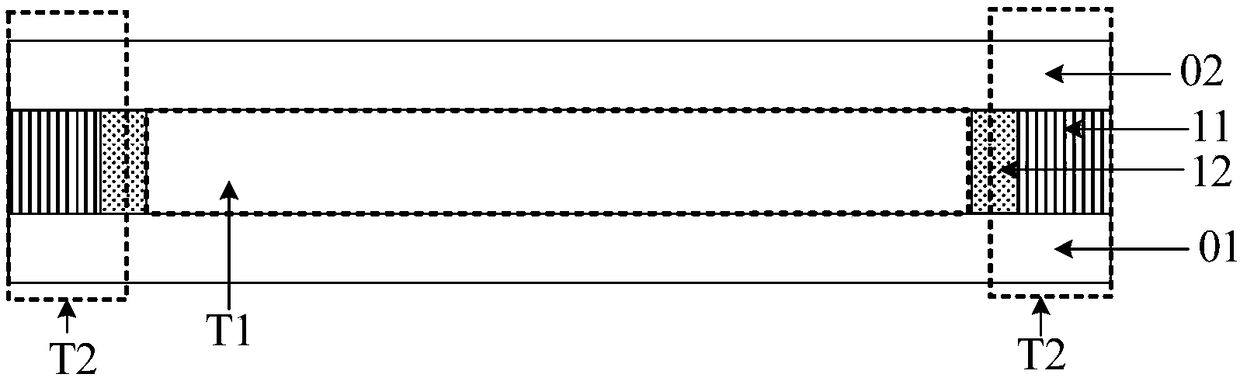
[0055]Figure 1A is a schematic structural diagram of a display panel provided by an embodiment of the present invention, as shown in Figure 1A As shown, the display panel may include: an array substrate 01 and an encapsulation cover 02 disposed opposite to each other.

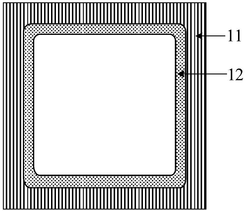
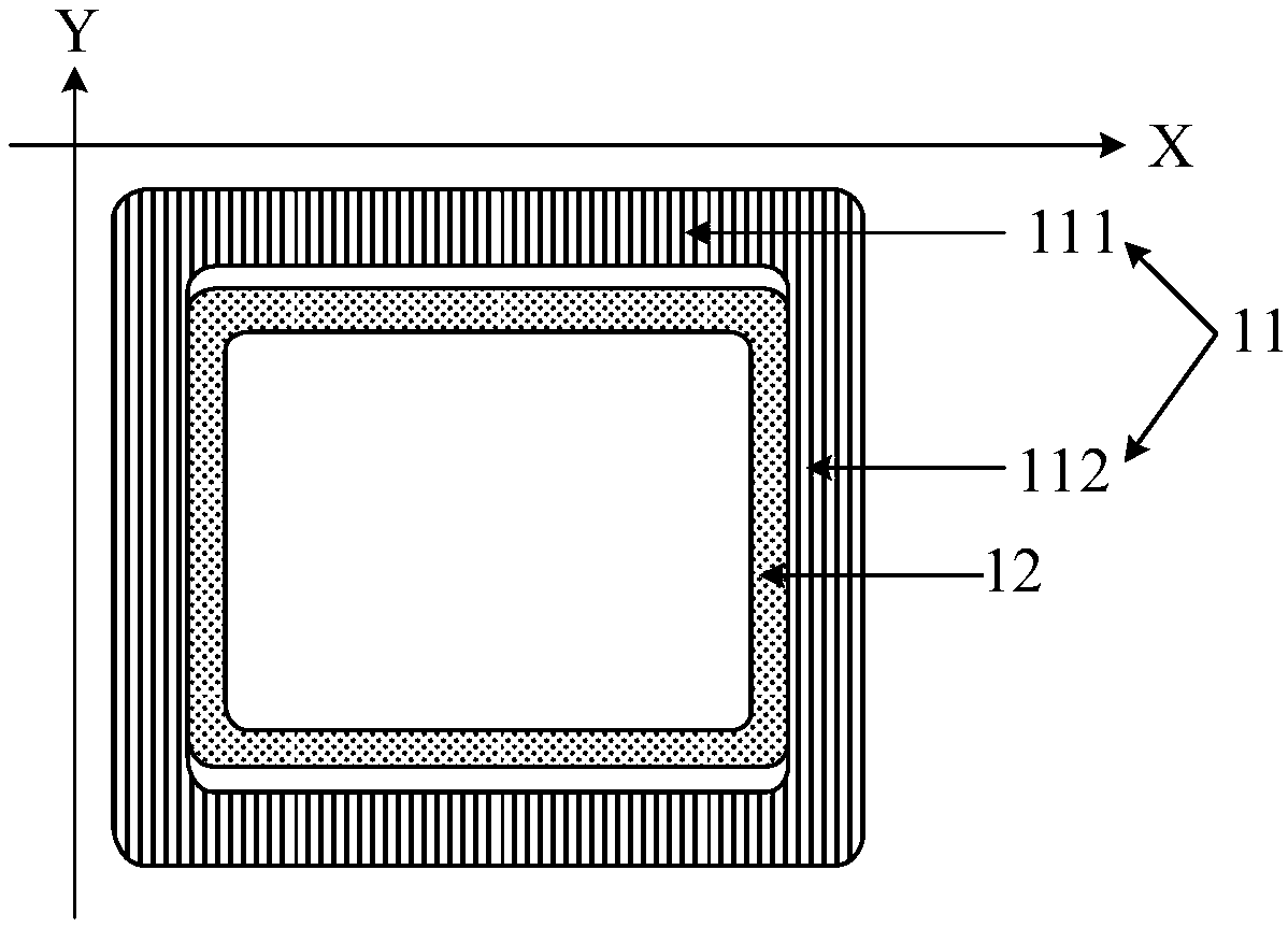
[0056] There is at least one target substrate in the array substrate 01 and the package cover 02 , for example, the target substrate in FIG. 1 may be the array substrate 01 . The target substrate has a display area T1 and a non-display area T2 surrounding the display area T1, and a support structure 11 may be disposed in the non-display area T2. The side of the support structure 11 close to the display area T1 is provided with an encapsulant 12 for encapsulating the ar...


PUM


Abstract

The invention discloses a display panel, a manufacturing method of the display panel and a display device, and belongs to the technical field of display. The display panel comprises an array substrateand a packaging cover plate which are oppositely arranged, at least one target substrate is arranged in the array substrate and the packaging cover plate, and the target substrate is provided with adisplay area and a non-display area; a supporting structure is arranged in the non-display area, and the side, away from the display area, of the supporting structure is coplanar with one side face ofthe array substrate or the packaging cover plate; the supporting structure is obtained from a cutting supporting structure in a display mother board when the display mother board is cut along a cutting line to form the display panel; the orthographic projection of the cutting supporting structure on the target substrate covers the area where the cutting line is located, so that when the display mother board is cut, the display mother board is cut along the cutting supporting structure, the problem that the stress of the display mother board is uneven due to cutting of other areas is avoided,and the appearance and quality of the display panel are ensured.

Description

technical field [0001] The present application relates to the field of display technology, in particular to a display panel, a manufacturing method thereof, and a display device. Background technique [0002] With the development of display technology, display panels formed by organic light emitting diodes (Organic Light Emitting Diode, OLED) have been widely used due to their characteristics of self-illumination, fast response and wide viewing angle. The luminescent material is easily affected by water or oxygen to produce oxidation reaction, so the display panel needs to be packaged when manufacturing the display panel. [0003] In the related art, cutting with glue is an effective technical means to realize a narrow frame. Therefore, when manufacturing the display panel, glass glue needs to be coated on the supporting area of ​​the display motherboard first, and the glass glue is irradiated with laser to make the glass glue harden. However, because the glass glue in the...

Claims


Application Information

Patent Timeline
Patent Type & Authority Applications(China)
IPC IPC(8): H01L51/56H01L51/52H01L27/32
CPCH10K59/00H10K50/84H10K71/851H10K71/00
Inventor 姜妮冯远明宋文华吴小会石博
Owner BOE TECH GRP CO LTD
Why Eureka
Try Eureka