OLED device

A device and platform technology, applied in the field of OLED devices, can solve the problems of OLED device quality degradation, affecting the microcavity effect, affecting the uniformity of light emission of OLED devices, etc., to achieve the goal of improving uniformity of light emission, uniform film formation, and smooth film surface Effect

Active Publication Date: 2018-09-28
SHENZHEN CHINA STAR OPTOELECTRONICS SEMICON DISPLAY TECH CO LTD
View PDF3 Cites 17 Cited by
  • Summary
  • Abstract
  • Description
  • Claims
  • Application Information

AI Technical Summary

Problems solved by technology

The unevenness of the organic functional layer will not only affect the uniformity of light emission of the OLED device, but also seriously affect the microcavity effect of the top emission (Top emission) OLED device, deteriorating the quality of the OLED device.

Method used


Image

  • OLED device
  • OLED device
  • OLED device

Examples


Embodiment Construction

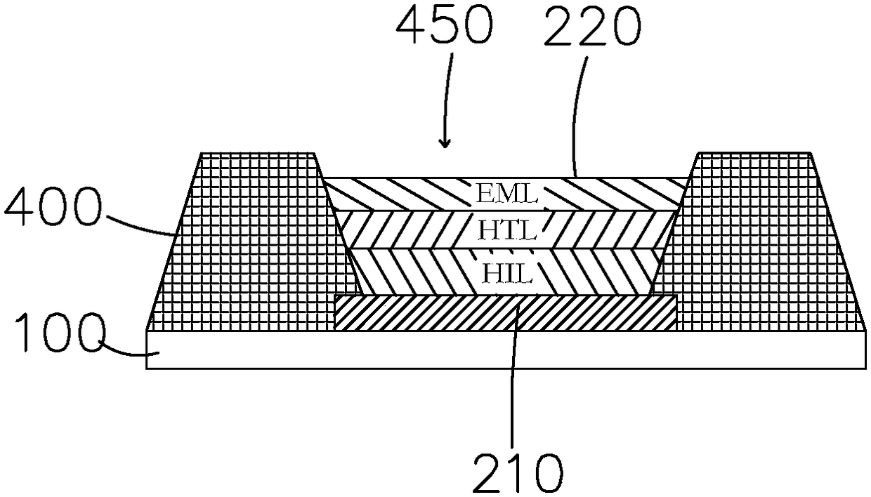
[0031] In order to further illustrate the technical means adopted by the present invention and its effects, the following describes in detail in conjunction with preferred embodiments of the present invention and accompanying drawings.

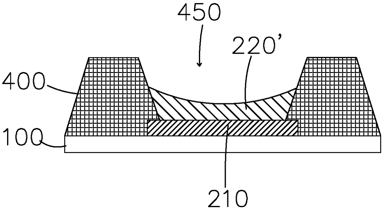
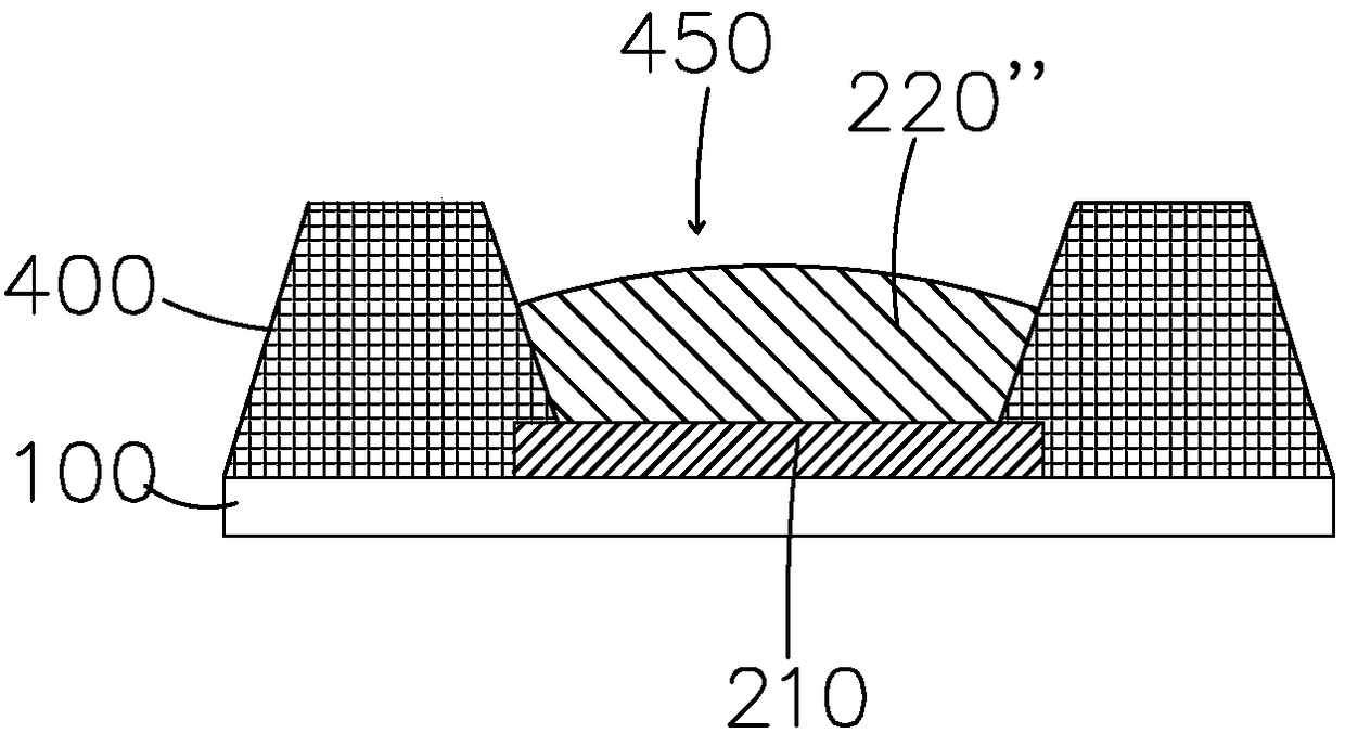
[0032] see Figure 4 , the present invention provides an OLED device, comprising a base substrate 10, an anode layer 21 disposed on the base substrate 10, a pixel definition layer 40 disposed on the base substrate 10 and the anode layer 21, and a pixel definition layer 40 disposed on the anode layer 21 The organic functional layer 22 and the cathode layer (not shown) arranged on the organic functional layer 22 and the pixel definition layer 40;

[0033] The pixel definition layer 40 includes a hydrophobic dam layer 41, and the hydrophobic dam layer 41 is provided with a plurality of step platforms 411 in a stepped shape, and the hydrophobic dam layer 41 passes through the plurality of step platforms 411 on the anode layer. A pixel opening are...


PUM


Abstract

The invention provides an OLED device, comprising a substrate, an anode layer, a pixel definition layer and an organic functional layer, wherein the pixel definition layer consists of a hydrophobic dam layer and a hydrophilic dam layer; a plurality of ladder-like step platforms are arranged on the hydrophobic dam layer; the hydrophobic dam layer defines a pixel opening area of which the upper partis wide and the lower part is narrow above the anode layer through the plurality of step platforms; and the hydrophilic dam layer is arranged on the upper surface of each step platform. Thereby, whenmanufacturing the organic functional layer by using an ink-jet printing technology, the film surface of an ink material that forms the organic functional layer can be leveled in the pixel opening area, and thus the uniform film formation of the organic functional layer in the pixel opening area can be achieved, the uniformity of luminance of the OLED device can be effectively improved, and the microcavity effect of top-emitting OLED devices can also be accurately controlled.

Description

technical field [0001] The invention relates to the field of display technology, in particular to an OLED device in which an organic functional layer is uniformly formed into a film. Background technique [0002] Organic Light Emitting Diodes (Organic Light Emitting Diodes, OLED) is a new type of current-mode semiconductor light-emitting device, which is a kind of autonomous light-emitting technology by controlling the injection and recombination of charge carriers in the device to excite organic materials to emit light. Compared with passive luminescent liquid crystal display (Liquid Crystal Display, LCD), self-luminous OLED display has the advantages of fast response, high contrast, wide viewing angle, etc., and it is easy to realize flexible display. It is generally optimistic in the industry, and the industry agrees that OLED display It is very likely to become the mainstream product of the next generation of display technology. [0003] OLEDs have an anode, an organic ...

Claims


Application Information

Patent Timeline
Patent Type & Authority Applications(China)
IPC IPC(8): H01L27/32H01L51/52H01L51/56
CPCH10K59/122H10K50/80H10K71/00
Inventor 邴一飞
Owner SHENZHEN CHINA STAR OPTOELECTRONICS SEMICON DISPLAY TECH CO LTD
Why Eureka
Try Eureka