Pixel circuit, drive method therefor, array substrate, and display device

A pixel circuit and array substrate technology, applied to static indicators, instruments, etc., can solve problems such as poor display effect of display devices

Active Publication Date: 2018-10-09
BOE TECH GRP CO LTD
View PDF14 Cites 10 Cited by
  • Summary
  • Abstract
  • Description
  • Claims
  • Application Information

AI Technical Summary

Problems solved by technology

[0005] The invention provides a pixel circuit and its driving method, an array substrate and a displa

Method used


Image

  • Pixel circuit, drive method therefor, array substrate, and display device
  • Pixel circuit, drive method therefor, array substrate, and display device
  • Pixel circuit, drive method therefor, array substrate, and display device

Examples


Embodiment Construction

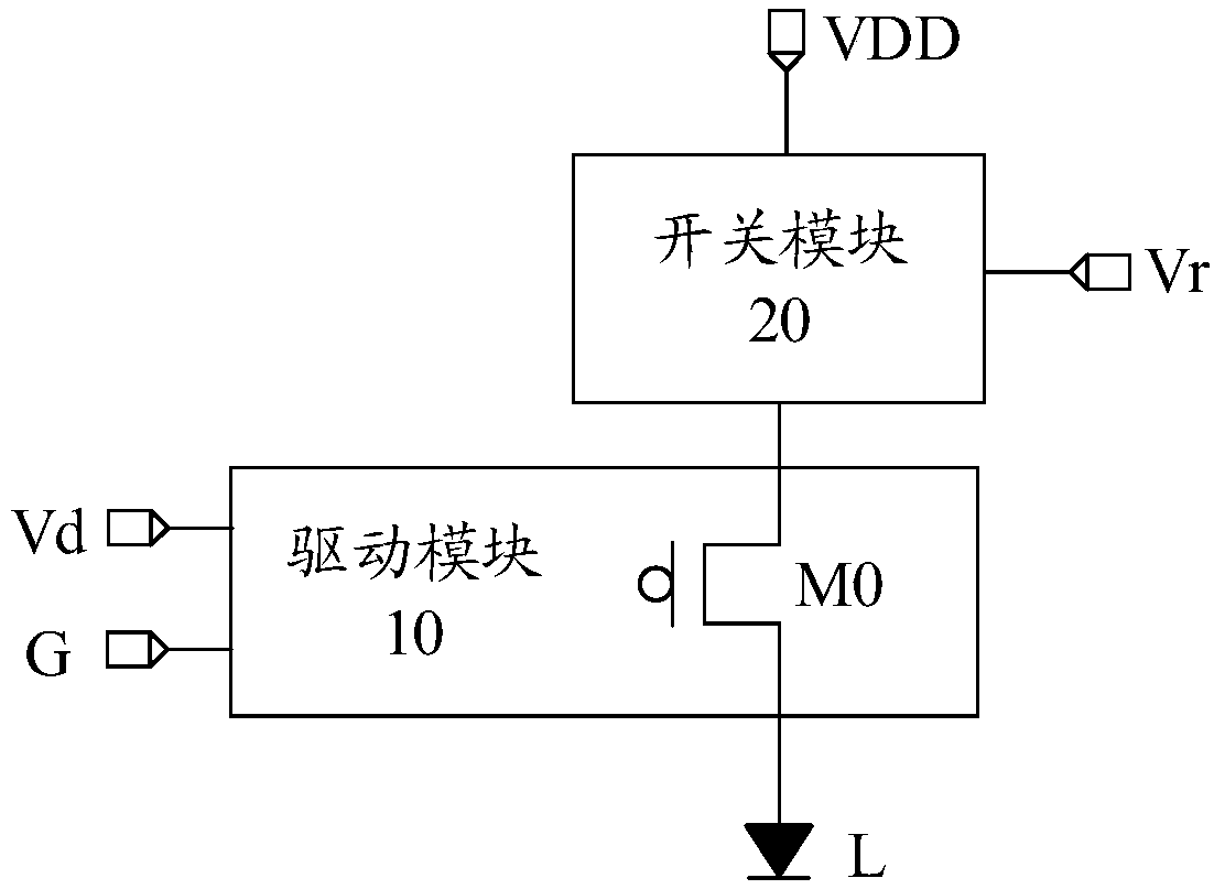
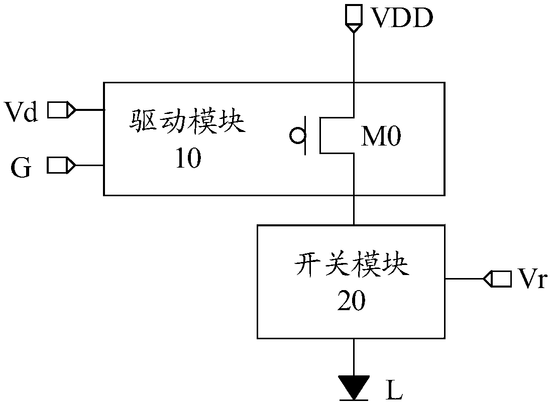
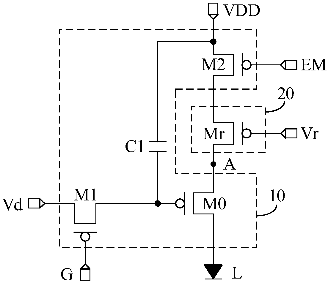
[0060] In order to make the object, technical solution and advantages of the present invention clearer, the implementation manner of the present invention will be further described in detail below in conjunction with the accompanying drawings.

[0061] The transistors used in all the embodiments of the present invention can be thin film transistors or field effect transistors or other devices with the same characteristics, and the transistors used in the embodiments of the present invention are mainly switching transistors according to their functions in circuits. Since the source and drain of the switching transistor used here are symmetrical, the source and drain are interchangeable. In the embodiment of the present invention, the source is referred to as the first stage, and the drain is referred to as the second stage. According to the form in the accompanying drawings, it is stipulated that the middle terminal of the transistor is the gate, the signal input terminal is th...


PUM


Abstract

The invention discloses a pixel circuit, a drive method therefor, an array substrate and a display device, and belongs to the technical field of display. The pixel circuit includes a drive module anda switch module, wherein the switch module is connected in series with a drive transistor in the drive module, and the switch module and the drive transistor in series connection are respectively connected with a power signal line and a light emitting unit. The drive module is also respectively connected with a gate line and a data line, and is used for providing a power signal from the power signal line for the light emitting unit through the drive transistor under the control of a gate drive signal provided by the gate line and a data signal provided by the data line. The switch module is also connected with a switching signal line, for controls the connection and disconnection between the power signal line and the light emitting unit under the control of a switching signal provided by the switching signal line. The pixel circuit provided by the invention can avoid dynamic smear when the display device displays a dynamic image, and the display device has a better display effect.

Description

technical field [0001] The present invention relates to the field of display technology, in particular to a pixel circuit and a driving method thereof, an array substrate and a display device. Background technique [0002] The pixel circuit is a circuit for driving OLED to emit light in an organic light emitting diode (Organic Light Emitting Diode, OLED) display device. [0003] In the related art, a pixel circuit generally includes a plurality of transistors and at least one capacitor. Among the plurality of transistors, there is a driving transistor, which can be used to control the magnitude of the current flowing through the OLED, thereby controlling the luminance of the OLED. The capacitor is connected to the gate of the driving transistor, and is used to maintain the gate voltage of the driving transistor, so that the driving transistor remains in an on state within one frame time, thereby ensuring that the OLED continues to emit light. [0004] However, when the disp...

Claims


Application Information

Patent Timeline
IPC IPC(8): G09G3/3266
CPCG09G3/3266G09G2320/0257G09G3/3233G09G2310/0262G09G2300/0861G09G2300/0819G09G2310/06G09G2320/0233G09G2310/0237G09G2320/0261G09G2320/103G09G3/3258G09G3/3275G09G2300/0852
Inventor 王铁石徐智强高雪岭羊振中
Owner BOE TECH GRP CO LTD
Why Eureka
Try Eureka