A layout method of decoder control circuit and nor Flash memory

A technology of control circuit and decoding circuit, which is applied in the direction of static memory, read-only memory, information storage, etc., can solve the problems of increasing peripheral drive circuit and control circuit area, large circuit layout area, and reducing reading speed, etc., so as to save logic Effects of complexity and layout area, simplified functional requirements, and increased read speed

Active Publication Date: 2021-03-26
XTX TECH INC
View PDF3 Cites 0 Cited by
  • Summary
  • Abstract
  • Description
  • Claims
  • Application Information

AI Technical Summary

Problems solved by technology

[0009] The purpose of the present invention is to provide a decoder control circuit in the prior art for the technical problems of complex structure, larger circuit layout area, lower reading speed, and increased area of ​​peripheral drive circuits and control circuits. The layout method of the circuit and the Nor Flash memory makes the decoder control circuit occupy a small layout area, the control principle and structure are simple, and the layout and wiring are simple, with strong reusability and easy scalability

Method used


Image

  • A layout method of decoder control circuit and nor Flash memory
  • A layout method of decoder control circuit and nor Flash memory
  • A layout method of decoder control circuit and nor Flash memory

Examples


Embodiment Construction

[0025] The decoder control circuit and the layout method of the Nor Flash memory provided by the present invention will be described in detail below in conjunction with the accompanying drawings. Apparently, the described embodiments are only some of the embodiments of the present invention, but not all of them. Based on the embodiments of the present invention, all other embodiments obtained by persons of ordinary skill in the art without making creative efforts belong to the protection scope of the present invention.

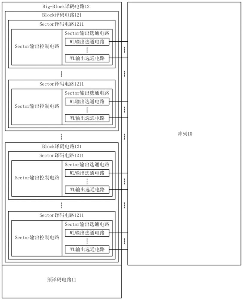
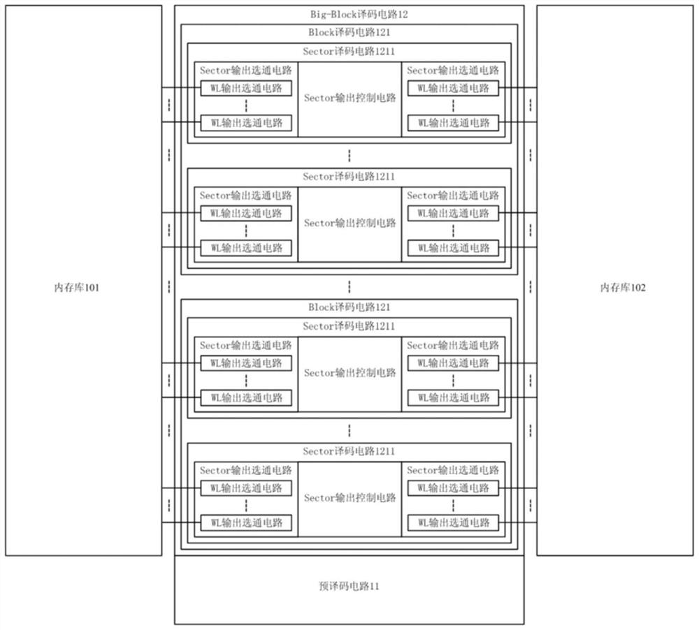
[0026] refer to image 3 , a schematic structural diagram of the decoder control circuit described in the present invention. The decoder control circuit is suitable for Nor Flash memory, and includes a pre-decoding circuit 31 and a Big-Block decoding circuit 32 . The pre-decoding circuit 31 is electrically connected with the Big-Block decoding circuit 32, and is used to decode the WL high-voltage signal in any mode of reading (Read), writing (PGM), and erasi...


PUM


Abstract

The invention discloses a decoder control circuit and a layout designing method for a Nor flash memory. The decoder control circuit is small in occupied layout area, simple in control principles and structure, uncomplicated in locating and wiring, small in the area of a peripheral drive circuit, short in reading path and fast in reading speed. In particular, the decoder control circuit of the invention has obvious area cost advantage, good reusability and easy expandability when applied to large-capacity Nor Flash memories prepared by using an advanced process.

Description

technical field [0001] The invention relates to the technical field of semiconductor memory chip design, in particular to a decoder control circuit used in a Nor Flash memory to save the decoder area of ​​a word line in an array and a layout method for a Nor Flash memory. Background technique [0002] The decoder control circuit (XDEC) in the non-volatile flash technology (Nor Flash) memory mainly provides the decoding of the word line (WL) for the memory array (Memory Array), and converts the read (Read), write (PGM), erase The voltage signal in (ER) and other modes is selected and output to the WL of the array cell (Array Cell) according to the mode control signal and address information, so XDEC is the only module circuit in the memory chip that increases linearly with the memory capacity. The smaller the process size of the Cell, the smaller the height of the Array, which limits the height of the XDEC on the layout. If the original circuit area remains unchanged, the X ...

Claims


Application Information

Patent Timeline
Patent Type & Authority Patents(China)
IPC IPC(8): G11C16/08
CPCG11C16/08
Inventor 李浩李军张小印马力
Owner XTX TECH INC
Why Eureka
Try Eureka