Array substrate and display device

An array substrate and array-type technology, applied in nonlinear optics, instruments, optics, etc., can solve the problems of limited increase in transmittance of liquid crystal display panels, difficulty in significantly improving transmittance, and small size of a single sub-pixel. Achieve the effects of improving longitudinal crosstalk, increasing transmittance, and increasing light transmission

Pending Publication Date: 2019-01-18
BOE TECH GRP CO LTD +1
View PDF14 Cites 8 Cited by
  • Summary
  • Abstract
  • Description
  • Claims
  • Application Information

AI Technical Summary

Problems solved by technology

However, the use of the above-mentioned high-transparency materials will not only increase the cost, but also limit the improvement of the transmittance of the liquid crystal display panel.
Especially for current high-resolution liquid crystal display devices such as 8K (7680×4320 resolution) and 10K (10240×4320 resolution), the size of a single sub-pixel is extremely small, and even if high-transparency materials are used, the transmittance is difficult to obtain. Significant improvement

Method used


Image

  • Array substrate and display device
  • Array substrate and display device
  • Array substrate and display device

Examples


Embodiment Construction

[0047] In order to make the above objects, features and advantages of the present invention more obvious and understandable, the technical solutions in the embodiments of the present invention will be clearly and completely described below in conjunction with the drawings in the embodiments of the present invention. Apparently, the described embodiments are only some of the embodiments of the present invention, but not all of them. Based on the embodiments of the present invention, all other embodiments obtained by persons of ordinary skill in the art without creative efforts fall within the protection scope of the present invention.

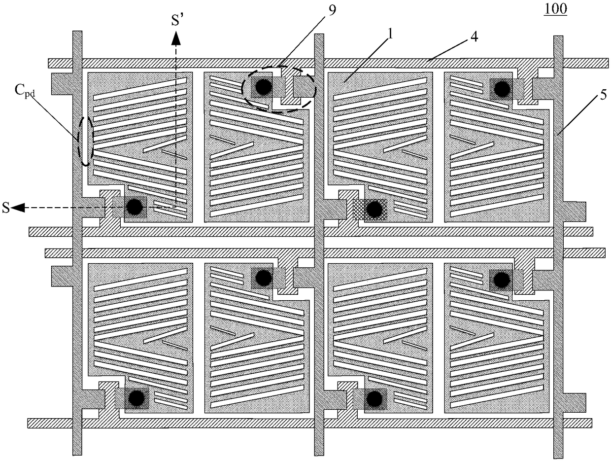
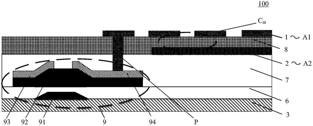
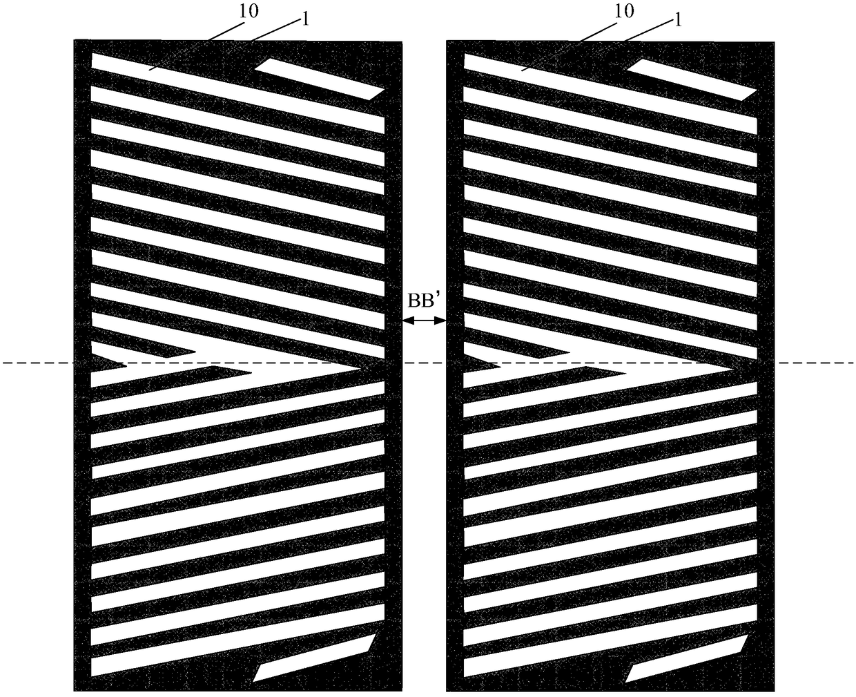
[0048] At present, in FFS (Fringe Field Switching, fringe field switching technology) display panels, the pixel structure in the array substrate adopts a single gate (Single Gate) structure or a double gate (Dual Gate) structure, and the dual gate pixel structure can effectively reduce the number of data lines. Quantity, thereby reducing the num...


PUM

PropertyMeasurementUnit
widthaaaaaaaaaa
widthaaaaaaaaaa

Abstract

The invention provides an array substrate and a display device, and relates to the technical field of display. The array substrate comprises a plurality of sub-pixels and a plurality of grid lines, wherein the plurality of sub-pixels are arranged in an array way, the plurality of sub-pixels in each line are electrically connected with two of the grid lines, the array substrate also comprises a substrate and a first electrode layer, the first electrode layer is arranged on the substrate and comprises a plurality of first electrodes, the plurality of first electrodes are in one-to-one correspondence to the plurality of sub-pixels, each first electrode comprises at least one first electrode unit, each first electrode unit comprises a plurality of strip-shaped electrodes and a connection electrode, the connection electrode is arranged at least one part of region around the plurality of strip-shaped electrodes, the plurality of strip-shaped electrodes are electrically connected with the connection electrode, the plurality of strip-shaped electrodes are arranged at intervals to form a plurality of gaps, and at least one position of the connection electrode is broken so that at least oneend of at least one gap forms in the breakage position of the connection electrode. When the array substrate is used in the display device, the transmittance of the display device can be improved.

Description

technical field [0001] The present invention relates to the field of display technology, in particular to an array substrate and a display device. Background technique [0002] A Liquid Crystal Display (LCD for short) relies on a backlight module disposed on the back of the LCD panel to provide light required for display, so the transmittance of the display panel is an important performance index thereof. With the development of display technology, the transmittance requirements of liquid crystal display panels are getting higher and higher. [0003] At the same time, in order to ensure a good display quality of the liquid crystal display panel, it is necessary to control defects such as black spots (Black Gap) and bright spots (such as blue spots (Blue Spot)) within a reasonable range. Among them, the reason for the formation of black spots is that the support density of the spacer in the liquid crystal display panel is not enough, resulting in the weak compressive capacit...

Claims


Application Information

Patent Timeline
Patent Type & Authority Applications(China)
IPC IPC(8): G02F1/1343G02F1/1362
CPCG02F1/134309G02F1/136209G02F2201/40G02F1/134372G02F1/133707G02F1/134345G02F1/136286
Inventor 王小元王武方琰白雅杰毕瑞琳
Owner BOE TECH GRP CO LTD
Why Eureka
Try Eureka