Array substrate, preparation method thereof and display panel

A technology of array substrate and delimiting layer, which is applied in semiconductor/solid-state device manufacturing, electrical components, electric solid-state devices, etc., can solve problems such as cathode layer faults, and achieve the effect of reducing the coffee ring effect

Active Publication Date: 2019-05-31
HEFEI BOE OPTOELECTRONICS TECH +1
View PDF4 Cites 10 Cited by
  • Summary
  • Abstract
  • Description
  • Claims
  • Application Information

AI Technical Summary

Problems solved by technology

[0003] The main purpose of the present invention is to provide an array substrate and its preparation method and a display panel, which are used to solve the coffee ring effect that occu

Method used


Image

  • Array substrate, preparation method thereof and display panel
  • Array substrate, preparation method thereof and display panel
  • Array substrate, preparation method thereof and display panel

Examples


preparation example Construction

[0063] Embodiments of the present invention provide a method for preparing an array substrate, see Figure 4 ,include:

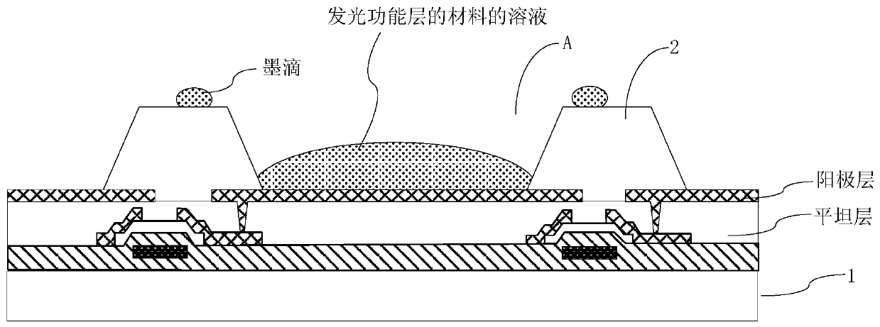
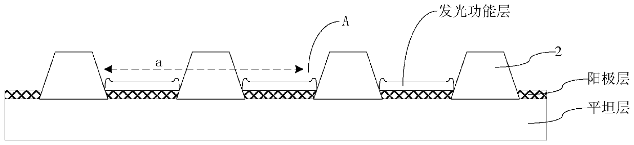
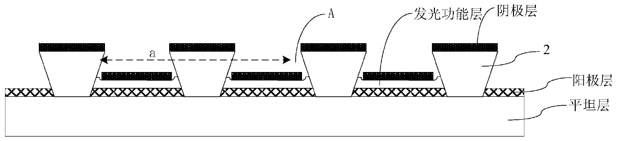
[0064] A pixel defining layer 2 is formed on a substrate 1, and the pixel defining layer 2 divides the substrate into a plurality of sub-pixel regions A. The pixel defining layer 2 includes a first defining layer 21 and a second defining layer 22 stacked in sequence from bottom to top, the width of the lower surface of the second defining layer 22 is greater than the width of the upper surface of the first defining layer 21, so that The two sides of the first defining layer 21 along the width direction form indented structures 23 relative to the second defining layer 22 .

[0065] On this basis, as Figure 4 As shown, before forming the pixel defining layer 2 on the substrate 1, the preparation method may further include sequentially forming a TFT (Thin Film Transistor, thin film transistor) array 6, a flat layer 7, an anode layer 4, etc. on the substrate ...


PUM

PropertyMeasurementUnit
Thicknessaaaaaaaaaa
Thicknessaaaaaaaaaa

Abstract

The invention relates to an array substrate, a preparation method thereof and a display panel, relates to the technical field of display, and aims at solving the problems of a coffee ring effect whena pixel definition layer uses a trapezoid structure and fault of a cathode layer when an inverted trapezoid structure is used. The array substrate comprises a substrate body and the pixel definition layer formed on the substrate body, the pixel definition layer divides the substrate body into sub-pixel areas, and comprises first and second definition layers arranged successively from bottom to topin a laminated way, and the lower surface of the second definition layer is wider than the upper surface of the first definition layer so that an indentation structure relative to the second definition layer is formed in the two sides of the first definition layer along the width direction. An OLED display panel is manufactured via an ink-jet printing technology according to embodiments of the invention.

Description

technical field [0001] The present invention relates to the field of display technology, in particular to an array substrate, a preparation method thereof, and a display panel. Background technique [0002] At present, the use of inkjet printing technology to make OLED (Organic Light-Emitting Diode, organic electroluminescent diode) display panels and QLED (Quantum Dot Light Emitting Diodes, quantum dot light-emitting diodes) display panels is the key to realize low-cost and large-area full-color The most efficient way to display. Contents of the invention [0003] The main purpose of the present invention is to provide an array substrate and its preparation method and a display panel, which are used to solve the coffee ring effect that occurs when the pixel defining layer adopts a trapezoidal structure in the related art, and the cathode layer fault that occurs when an inverted trapezoidal structure is adopted. The problem. [0004] To achieve the above object, the pres...

Claims


Application Information

Patent Timeline
IPC IPC(8): H01L27/32H01L51/56H01L51/00
Inventor 宫奎段献学张志海尹洋植
Owner HEFEI BOE OPTOELECTRONICS TECH
Why Eureka
Try Eureka