Display device and manufacturing method thereof

A display device and encapsulation layer technology, which is applied to identification devices, instruments, semiconductor devices, etc., can solve the problems affecting the display quality of Micro-LED display devices and the inability to achieve high resolution, so as to improve display performance and service life, and improve Display performance, effect of improving working life

Pending Publication Date: 2022-03-08
SHANGHAI TIANMA MICRO ELECTRONICS CO LTD
View PDF0 Cites 0 Cited by
  • Summary
  • Abstract
  • Description
  • Claims
  • Application Information

AI Technical Summary

Problems solved by technology

[0004] However, at present, there is no suitable TFT AM (Thin Film Transistor Active Matrix) driving circuit and driving method for Mini / Micro-LED at this stage, and the stability of TFT also seriously affects the display quality of Micro-LED display devices, and PM (Passive Matrix) The drive method cannot achieve high resolution

Method used


Image

  • Display device and manufacturing method thereof
  • Display device and manufacturing method thereof
  • Display device and manufacturing method thereof

Examples


Embodiment Construction

[0042] The following will clearly and completely describe the technical solutions in the embodiments of the present invention with reference to the accompanying drawings in the embodiments of the present invention. Obviously, the described embodiments are only some, not all, embodiments of the present invention. Based on the embodiments of the present invention, all other embodiments obtained by persons of ordinary skill in the art without making creative efforts belong to the protection scope of the present invention.

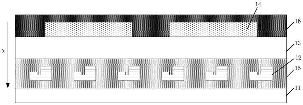
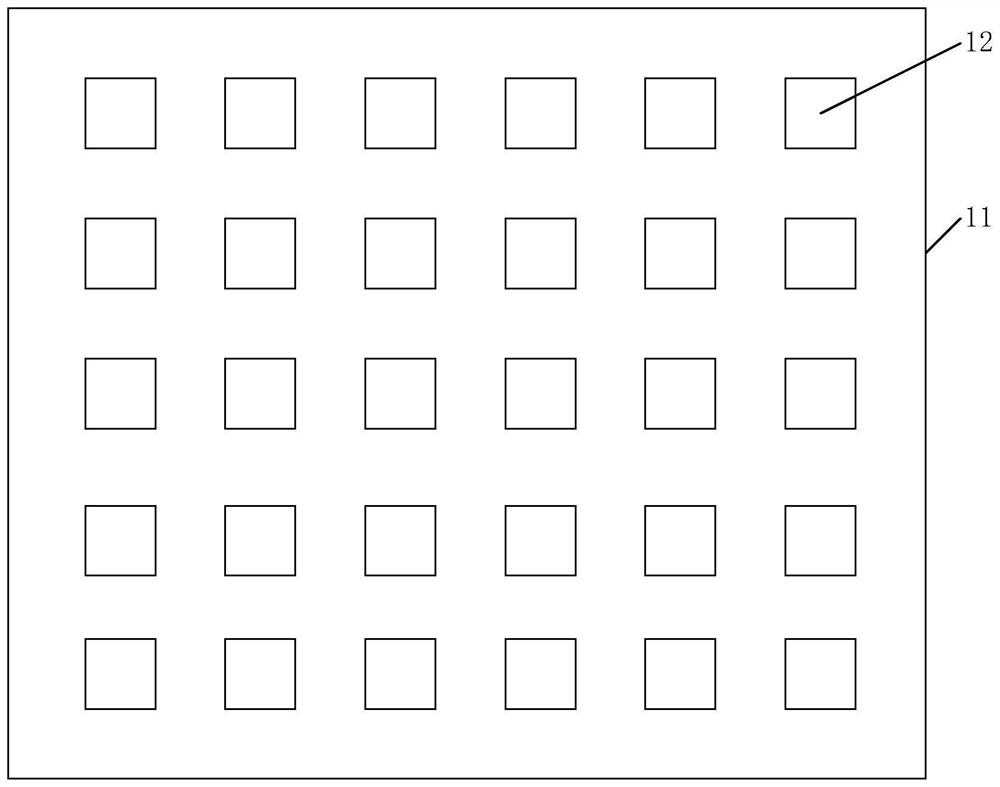
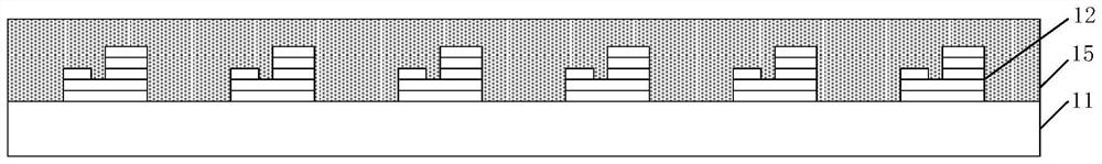
[0043] Based on the content described in the background technology, during the invention and creation process of this application, the inventor found that the current Micro-LED display devices all use Micro-IC to drive one pixel unit or several pixel units, so the micron-scale Micro-IC must be distributed between the pixel units.

[0044] If the Micro-IC is distributed among the pixel units, since it will occupy a part of the pixel area, it will also affect th...


PUM


Abstract

According to the display device and the manufacturing method thereof, the first chip and the light-emitting unit in the display device are located on the two sides of the wiring layer, packaging of the light-emitting unit is achieved through the first packaging layer, packaging of the first chip is achieved through the second packaging layer, heat dissipation of the first chip and heat dissipation of the light-emitting unit do not conflict, and therefore the heat dissipation efficiency of the display device is improved. The influence of heat emitted by the first chip in the working process on the working state of the light-emitting unit is reduced, so that the working life of the light-emitting unit is prolonged, the display performance of the display device is improved, and the service life of the display device is prolonged. Moreover, since the first chip and the light-emitting unit are located on the two sides of the wiring layer, the first chip does not occupy the area of the film layer where the light-emitting unit is located obviously, that is, the pixel area of the display device is not affected, and the display performance of the display device can be improved.

Description

technical field [0001] The present invention relates to the field of display technology, and more specifically, to a display device and a manufacturing method thereof. Background technique [0002] Micro-LED, also known as Micro Light Emitting Diode (Micro Light Emitting Diode), is following Liquid Crystal Display (LCD for short) and Active-Matrix Organic Light-Emitting Diode (AMOLED). A self-luminous device applied to next-generation display device technology. [0003] The core technology of the Micro-LED display device is to combine and arrange millions to tens of millions of LED chips with a size of tens of microns to form each pixel required by the display device. [0004] However, at present, there is no suitable TFT AM (Thin Film Transistor Active Matrix) driving circuit and driving method for Mini / Micro-LED at this stage, and the stability of TFT also seriously affects the display quality of Micro-LED display devices, and PM (Passive Matrix) The drive method cannot ...

Claims


Application Information

Patent Timeline
Patent Type & Authority Applications(China)
IPC IPC(8): H01L25/075H01L33/54H01L33/62G09F9/33
CPCH01L25/0753H01L33/54H01L33/62G09F9/33
Inventor 戴文君秦锋丁渊鄢杰林张灿源
Owner SHANGHAI TIANMA MICRO ELECTRONICS CO LTD
Why Eureka
Try Eureka