Supercharge Your Innovation With Domain-Expert AI Agents!

Semiconductor device for performing an error check operation

a technology of mikro-conductor and error check operation, which is applied in error detection/correction, digital storage, instruments, etc., can solve the problem of increasing the probability of an error to occur during a data transmission process

Active Publication Date: 2022-01-11
SK HYNIX INC
View PDF7 Cites 0 Cited by
  • Summary
  • Abstract
  • Description
  • Claims
  • Application Information

AI Technical Summary

Problems solved by technology

In the case where an input / output speed of data is increased, the probability of an error to occur during a data transmission process also increases.

Method used


Image

  • Semiconductor device for performing an error check operation
  • Semiconductor device for performing an error check operation
  • Semiconductor device for performing an error check operation

Examples


Embodiment Construction

[0015]Hereinafter, a semiconductor device will be described below with reference to the accompanying drawings through various examples of embodiments.

[0016]Various embodiments may be directed to a semiconductor device which generates a signal for performing a burst chop operation from a command address in a read operation and performs in parallel the burst chop operation and an error check operation.

[0017]According to the embodiments of the disclosure, it may be possible to provide a semiconductor device which generates a signal for performing a burst chop operation from a command address in a read operation and performs in parallel the burst chop operation and an error check operation.

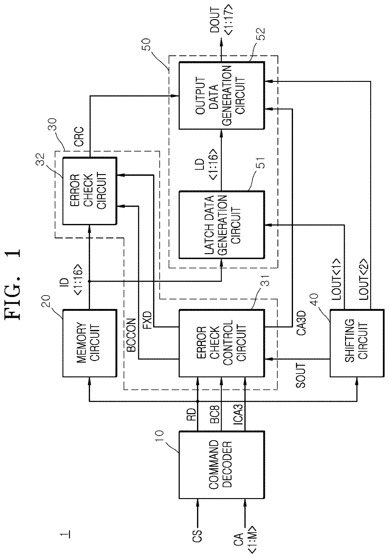
[0018]As illustrated in FIG. 1, a semiconductor device 1 in accordance with an embodiment of the disclosure may include a command decoder 10, a memory circuit 20, an error detection circuit 30, a shifting circuit 40 and a data output circuit 50.

[0019]The command decoder 10 may decode a chip select sig...


PUM


Abstract

A semiconductor device includes an error detection circuit configured to generate fixed data by fixing any one of a first group and a second group included in internal data to a preset level based on a burst chop signal and an internal command address in response to a read command, and generate an error detection signal by detecting an error of the fixed data; and a data output circuit configured to generate latch data by latching the internal data based on a first latch output control signal, and generate output data by serializing the latch data and the error detection signal based on a second latch output control signal.

Description

CROSS-REFERENCE TO RELATED APPLICATION[0001]The present application claims priority under 35 U.S.C. § 119(a) to Korean Patent Application No. 10-2019-0025317 filed on Mar. 5, 2019 in the Korean Intellectual Property Office, which is incorporated herein by reference in its entirety.BACKGROUND1. Technical Field[0002]Embodiments of the disclosure may generally relate to a semiconductor device configured for performing an error check operation.2. Related Art[0003]Recently, in order to increase the operating speed of a semiconductor device, a scheme of inputting / outputting a plurality of data in each clock cycle is used. In the case where an input / output speed of data is increased, the probability of an error to occur during a data transmission process also increases. Therefore, a separate device and method for ensuring the reliability of data transmission are additionally demanded.[0004]There is used a method of generating error codes capable of checking the occurrence of an error and t...

Claims


Application Information

Patent Timeline
Patent Type & Authority Patents(United States)
IPC IPC(8): G06F11/00G06F11/07G11C7/22G11C7/10G11C8/10
CPCG06F11/0751G06F11/0727G06F11/0772G11C7/106G11C7/222G11C8/10G06F11/1048G11C29/42G11C7/1006G06F11/1004G11C7/22
Inventor CHOI, GEUN HOCHOI, SUN MYUNG
Owner SK HYNIX INC
Features
  • R&D
  • Intellectual Property
  • Life Sciences
  • Materials
  • Tech Scout
  • Unparalleled Data Quality
  • Higher Quality Content
  • 60% Fewer Hallucinations
Learn More