

Semiconductor device and method of manufacturing the same
a semiconductor and oxide film technology, applied in the direction of semiconductor devices, basic electric elements, electrical appliances, etc., can solve the problems of increasing leakage current, reducing and increasing the stress to be produced around trench isolation, so as to prevent the reliability of semiconductor devices from degraded
- Summary
- Abstract
- Description
- Claims
- Application Information
AI Technical Summary
Benefits of technology
Problems solved by technology
Method used
Image

Examples
first preferred embodiment
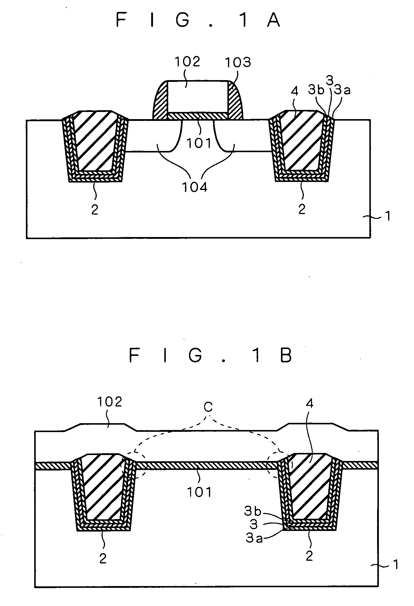
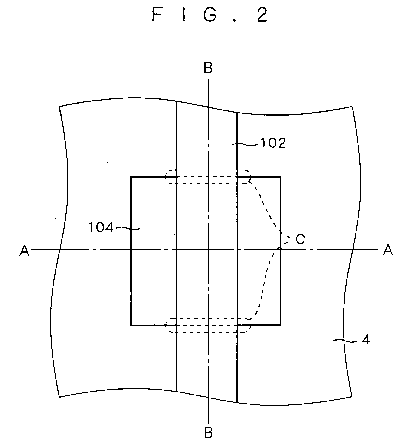
[0024]FIGS. 1A, 1B and 2 show the structure of a semiconductor device according to a first preferred embodiment of the present invention. FIGS. 1A and 1B are both sectional views of a MOS transistor, and FIG. 2 is a top view thereof. FIG. 1A corresponds to a section taken along the line A-A (i.e., along the gate length) shown in FIG. 2, and FIG. 1B corresponds to a section taken along the line B-B (i.e., along the gate width). In these drawings, the same elements are indicated by the same reference characters.
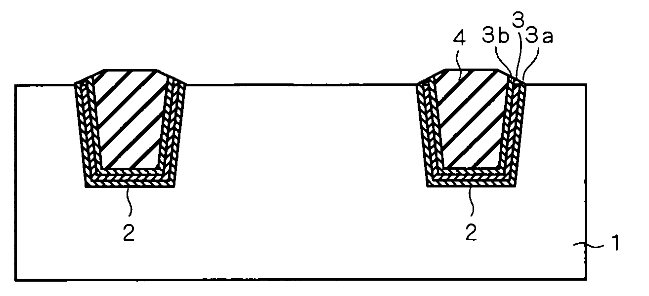
[0025] As shown in FIGS. 1A and 1B, formed in a silicon substrate 1 is a MOS transistor made up of a gate oxide film 101, a gate electrode 102, a sidewall 103 and source / drain regions 104. An active region (element forming region) where the MOS transistor is formed is defined by a trench isolation including a trench 2 formed in an element isolation region and an isolation oxide film 4 which fills the trench 2.
[0026] An inner wall oxide film 3 is formed on the inner wall of th...
second preferred embodiment
[0044] In the method of manufacturing a semiconductor device according to the present invention, the step of introducing nitrogen into the inner wall of the trench 2 on which the inner wall oxide film 3 is formed is conducted twice. For instance, in the first preferred embodiment, the inner wall oxide film 3 is first formed on the inner wall of the trench 2, and then, the two steps of introducing nitrogen (the first step of introducing nitrogen into a relatively deep position and the second step of introducing nitrogen into a relatively shallow position) are conducted.
[0045] According to the present invention, however, the two steps of introducing nitrogen do not always need to be conducted after forming the inner wall oxide film 3. In a second preferred embodiment, one of the first and second steps is conducted before forming the inner wall oxide film 3.
[0046] More specifically, in the method of manufacturing a semiconductor device according to the present embodiment, a first ste...
third preferred embodiment
[0052] In the present embodiment, a specific example to which the present invention is applied effectively will be described.
[0053]FIG. 8 shows the structure of a semiconductor device according to a third preferred embodiment, illustrating the cross-section of a memory cell region and a peripheral circuit region of a flash memory device. More specifically, the left half illustrates the cross-section of a transistor in the memory cell region (hereinafter referred to as a “memory transistor”) taken along the gate width, and the right half illustrates the cross section of a transistor of a peripheral circuit (hereinafter referred to as a “peripheral transistor”) taken along the gate width.
[0054] As shown in FIG. 8, an element isolation structure similar to that described in the first preferred embodiment (see FIGS. 1A and 1B) is formed in the memory cell region and peripheral circuit region of the semiconductor device. More specifically, the isolation oxide film 4 which defines activ...
PUM
 Abstract
Description
Claims
Application Information