Display device

a technology of a display device and a display screen, which is applied in the direction of discharge tube main electrodes, discharge tube screens, discharge tubes with screens, etc., can solve the problems of damage or degrade electron emission elements or fluorescent screens, electrical discharge (dielectric breakdown) between the substrates, and the gap between front and rear substrates cannot be greatly expanded, etc., to achieve excellent display quality, enlarge the discharge scale, and destroy the effect of circuits

Inactive Publication Date: 2007-07-19
KK TOSHIBA
View PDF5 Cites 0 Cited by
  • Summary
  • Abstract
  • Description
  • Claims
  • Application Information

AI Technical Summary

Benefits of technology

[0013] The present invention has been made in light of the above. An object of the invention is to provide an excellent display quality display device in which enlargement of the scale of discharge is suppressed, and destruction / degradation of electron emission elements and fluorescent screen, and destruction of circuits are suppressed.

Problems solved by technology

However, in view of the resolution, the properties of the support members, etc., the gap between the front and rear substrates cannot be greatly enlarged, and need to be set to about 1 to 2 mm.
Accordingly, in FEDs, a strong electric field will inevitably occur in the small gap between the front and rear substrates, thereby causing electrical discharge (dielectric breakdown) between the substrates.
When electrical discharge occurs, a current of 100 A or more may instantaneously flow, which may damage or degrade electron emission elements or fluorescent screen, and may even destroy driving circuits.
However, it is very difficult to completely suppress discharge over a long period.
Thus, it is difficult to suppress enlargement of the scale of discharge.

Method used


Image

  • Display device
  • Display device
  • Display device

Examples


Embodiment Construction

[0026] An embodiment, in which the display device of the invention is applied to an SED, will be described in detail with reference to the accompanying drawings.

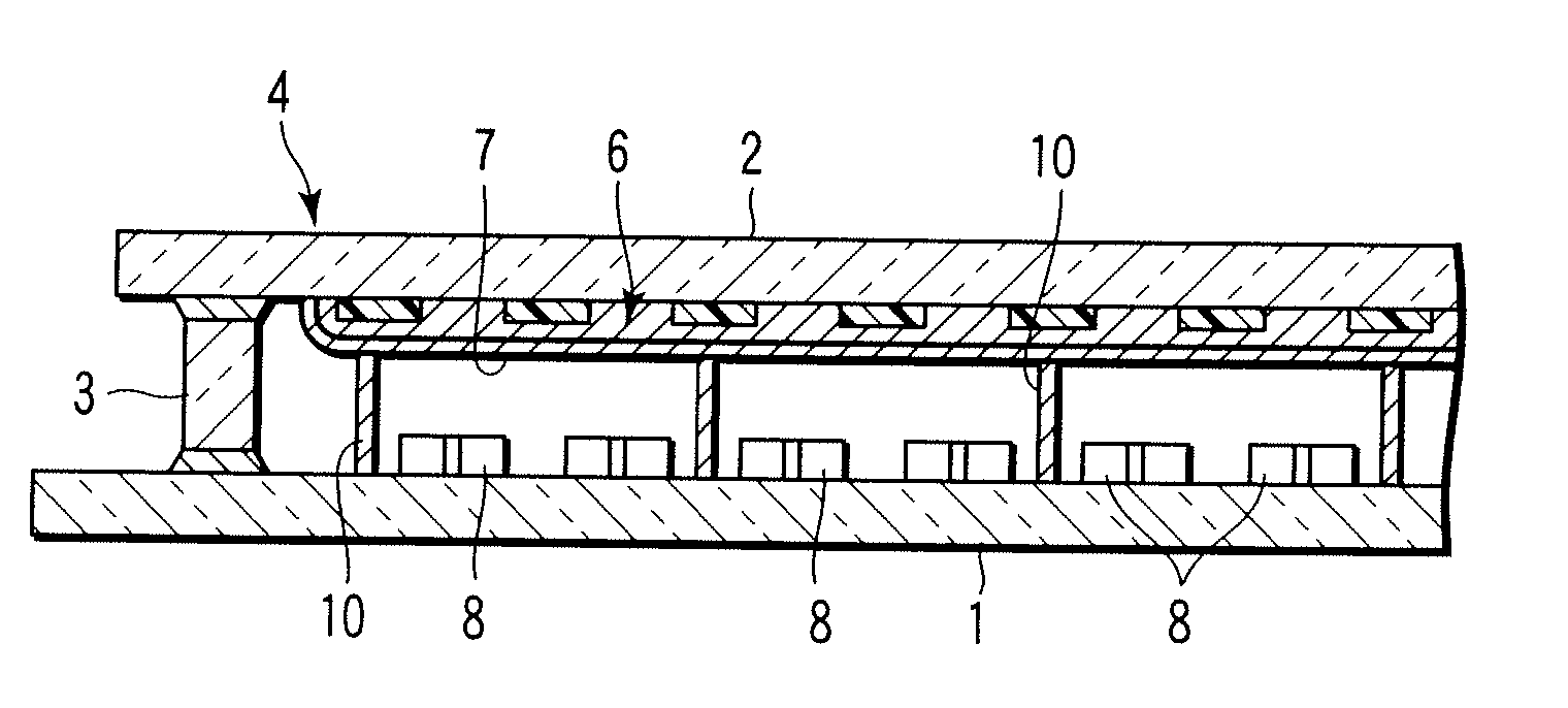
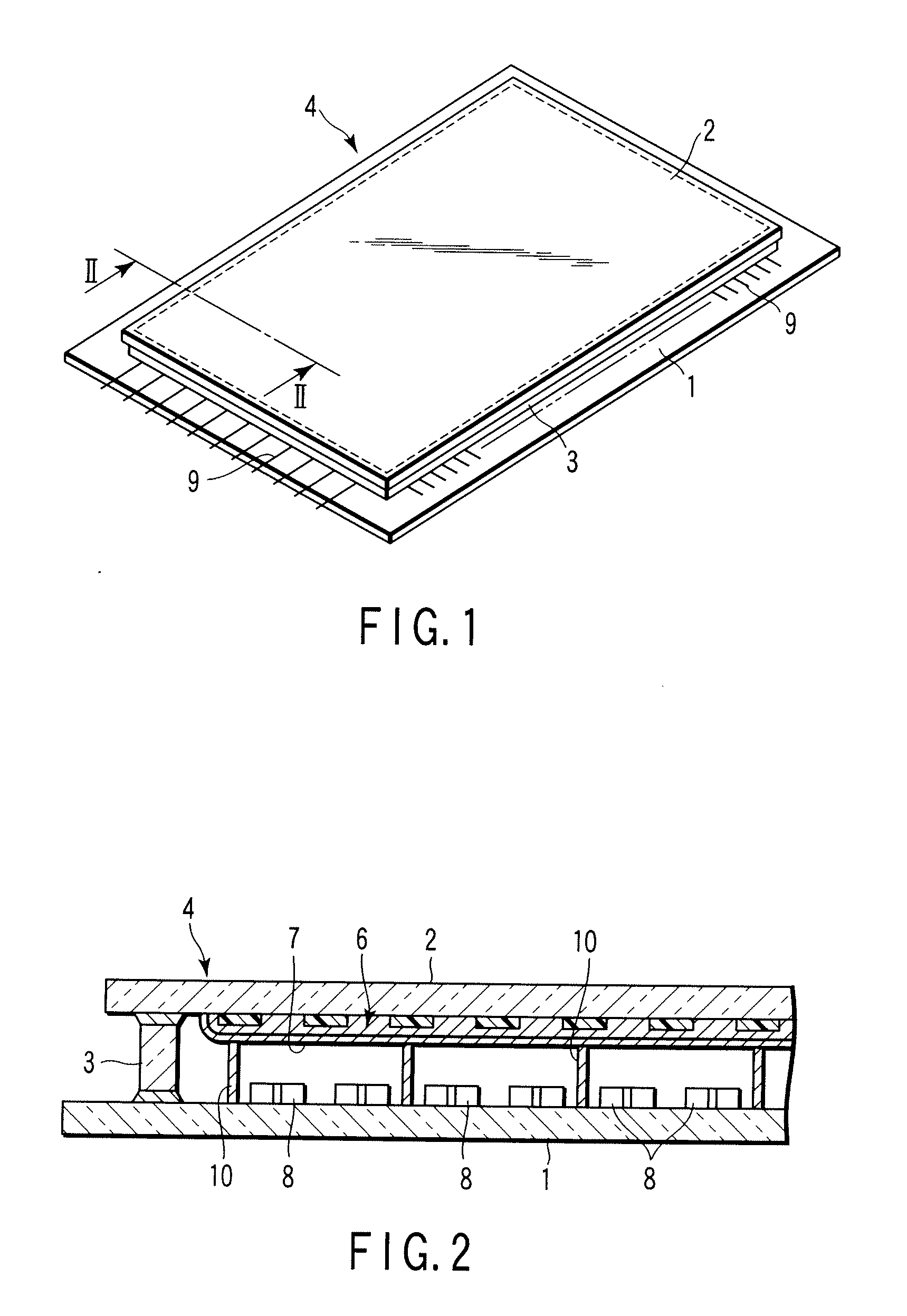
[0027] As shown in FIGS. 1 and 2, the SED comprises a front substrate 2 and rear substrate 1 formed of rectangular glass members. The front and rear substrates 2 and 1 are arranged opposite to each other with a gap of 1 to 2 mm therebetween. The front and rear substrates 2 and 1 have their peripheries bonded to each other via a rectangular frame-shaped side wall 3, thereby forming a flat, rectangular vacuum envelope 4 having its interior highly evacuated to about 10−4 Pa or less.

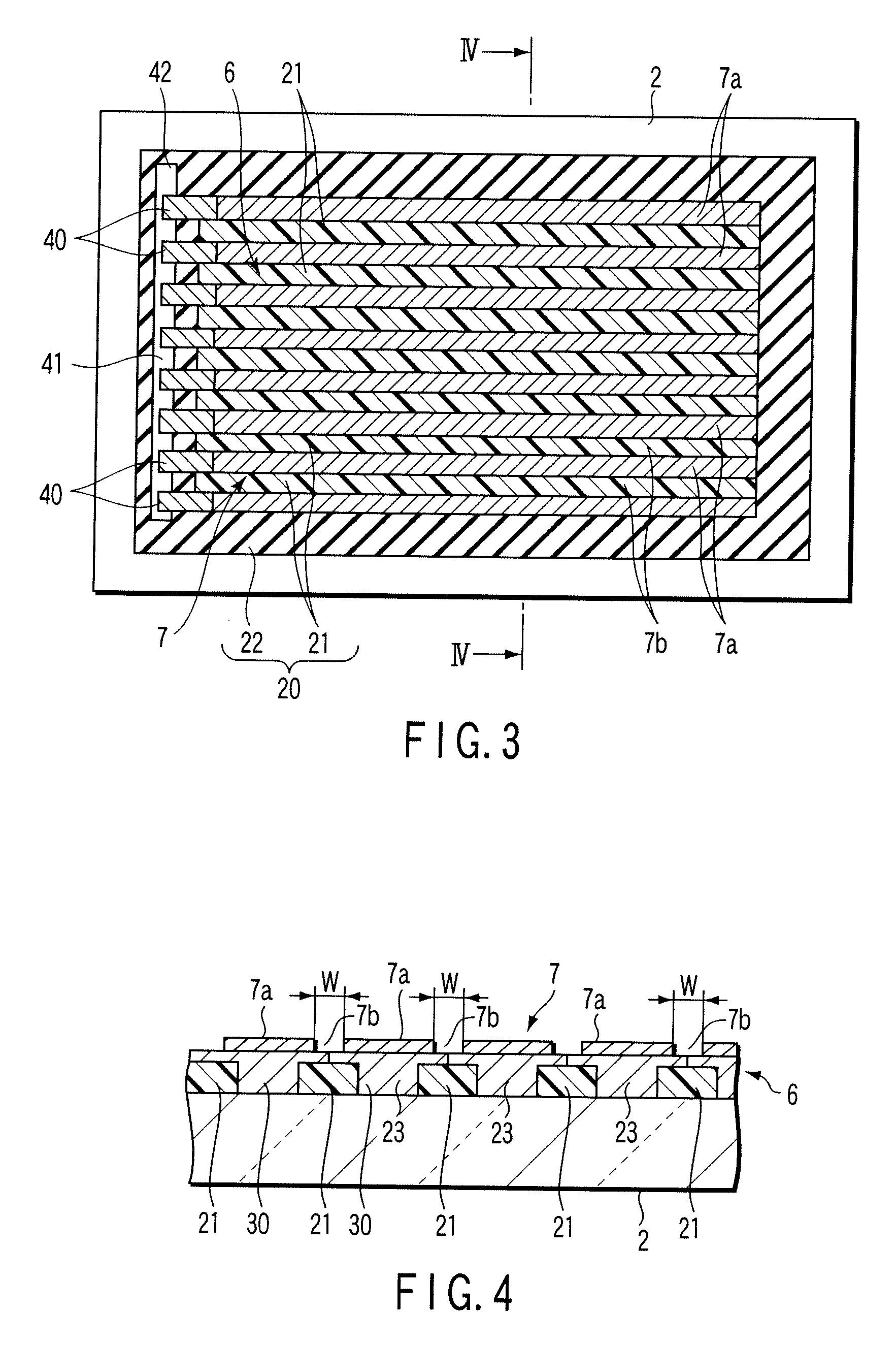
[0028] A fluorescent screen 6 is provided on the inner surface of the front substrate 2. The fluorescent screen 6 is formed of fluorescent layers that emit red, green and blue beams, and a shading layer. A metal-back layer 7 serving as an anode electrode is formed on the fluorescent screen 6. During a display operation, a predetermined anode voltag...


PUM


Abstract

A display device comprises a fluorescent screen provided with a shading portion including a plurality of openings, and a fluorescent layer formed on the shading portion, and a metal-back layer provided on the fluorescent screen and including a plurality of dividing means and a plurality of divisions defined by the dividing means, wherein the dividing means are provided on the shading portion via the fluorescent layer interposed therebetween, and an electrical resistance between each pair of adjacent ones of the divisions located with a corresponding dividing means interposed between the each pair falls within a range of 102Ω to 105Ω via the fluorescent layer.

Description

CROSS-REFERENCE TO RELATED APPLICATIONS [0001] This is a Continuation Application of PCT Application No. PCT / JP2005 / 011529, filed Jun. 23, 2005, which was published under PCT Article 21(2) in Japanese. [0002] This application is based upon and claims the benefit of priority from prior Japanese Patent Application No. 2004-198254, filed Jul. 5, 2004, the entire contents of which are incorporated herein by reference.BACKGROUND OF THE INVENTION [0003] 1. Field of the Invention The present invention relates to a display device. [0004] 2. Description of the Related Art In recent years, flat-panel display devices, in which a large number of electron emission elements are opposed to a fluorescent screen, have been developed as display devices. Various electron emission elements now available fundamentally utilize field emission. For instance, a field emission display (hereinafter referred to as an “FED”) for emitting electron beams from its electron emission elements to cause a fluorescent ...

Claims


Application Information

Patent Timeline
Patent Type & Authority Applications(United States)
IPC IPC(8): H01J63/04H01J1/62
CPCH01J31/127H01J29/28H01J1/30H01J31/12
Inventor KOZUKA, TOMOKOTANAKA, HAJIMENAKAMURA, AKIYOSHIMIKAMI, AKIRAITO, TAKEO
Owner KK TOSHIBA
Why Eureka
Try Eureka