Image display apparatus, correction circuit thereof and method for driving image display apparatus

Inactive Publication Date: 2009-09-03
CANON KK
View PDF27 Cites 3 Cited by
  • Summary
  • Abstract
  • Description
  • Claims
  • Application Information

AI Technical Summary

Benefits of technology

[0008]In the image display apparatus, a signal loss such as a voltage drop deteriorates the quality of the image displayed. Efforts have

Problems solved by technology

In the image display apparatus, a signal loss such as a vo

Method used


Image

  • Image display apparatus, correction circuit thereof and method for driving image display apparatus
  • Image display apparatus, correction circuit thereof and method for driving image display apparatus
  • Image display apparatus, correction circuit thereof and method for driving image display apparatus

Examples


first embodiment

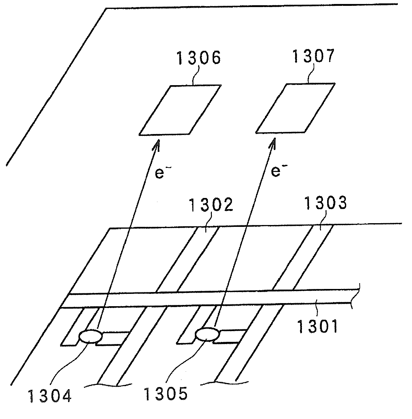
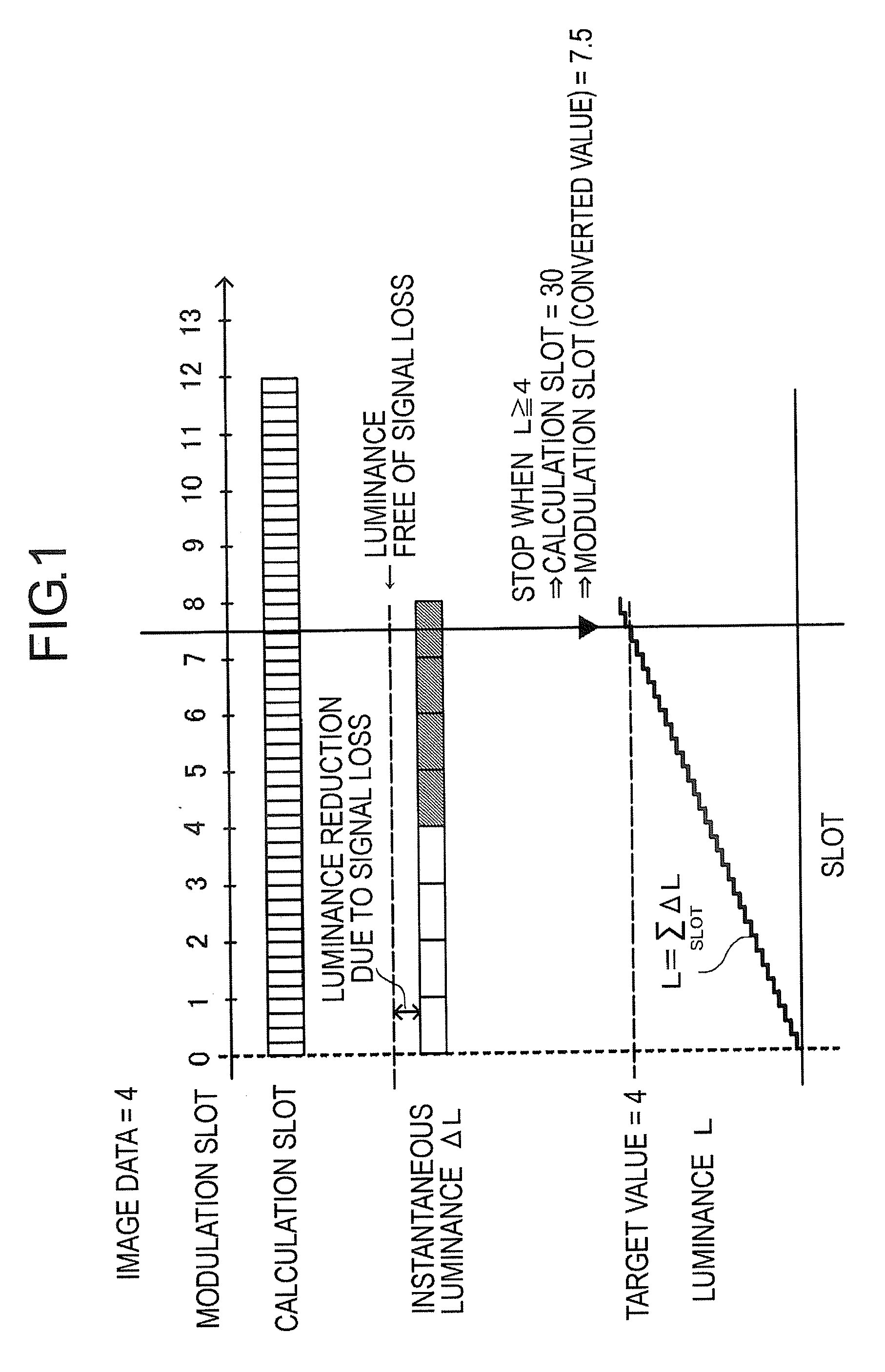
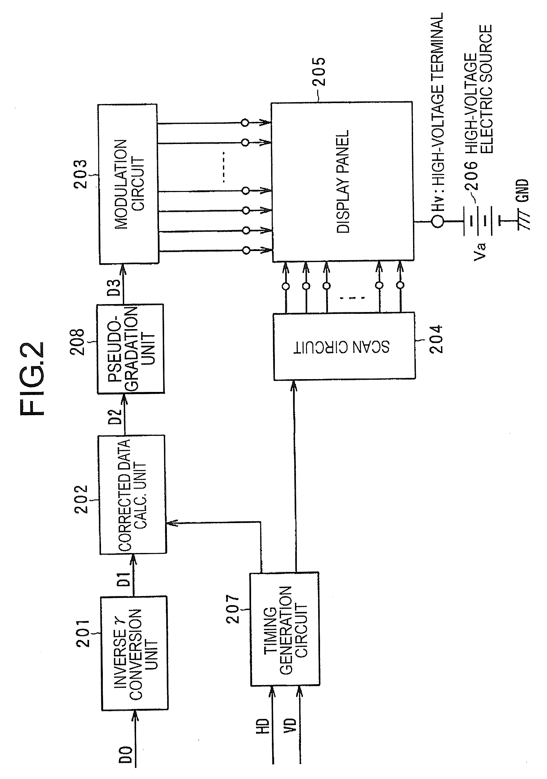
[0060]The image display apparatus according to the first embodiment generally includes a display panel with plural surface conduction electron-emitting devices arranged in simple matrix, a driving circuit (scan circuit, modulation circuit) for driving the display panel, and a correction circuit. According to this embodiment, the driving circuit drives the row wirings (scan wirings) in line sequence and applies the modulation pulse in which at least a pulse width is modulated to the column wirings (modulation wirings). The lighting time of each device is controlled by the pulse width. In addition to the lighting time control by the pulse width modulation (PWM), the lighting strength within a lighting period is desirably controlled by the pulse height modulation (PHM). In the description that follows, however, only the pulse width modulation is shown as an example to facilitate the understanding.

[0061]In the image display apparatus according to this embodiment, the input image data is...

second embodiment

[0128]In the first embodiment, as shown in FIG. 9, the luminance accumulation circuit is arranged for each column wiring. According to the second embodiment, in contrast, plural column wirings are divided into plural blocks, and the luminance accumulation circuit is arranged for each block. By executing the process block by block, the corrected data can be calculated quickly while at the same time making it possible to reduce the circuit size advantageously.

[0129]FIG. 7 is a diagram showing the configuration of the image display apparatus according to a second embodiment. The second embodiment is different from the first embodiment in that the corrected data calculation unit 202 is replaced by a discrete corrected data calculation unit 703 and a biaxial interpolation circuit 704. In this case, the discrete corrected data calculation unit 703, the biaxial interpolation circuit 704 and the pseudo-gradation unit 208 make up the correction circuit. The other parts of the configuration a...


PUM


Abstract

A correction circuit includes a timing control circuit for dividing a drive period assigned for drive of display devices into plural calculation slots, a luminance calculation circuit for calculating luminance including an effect of a voltage drop for each calculation slot, an accumulation circuit for temporally accumulating the luminance for each calculation slot, a corrected data determination circuit for outputting, as a corrected data, the value determined in accordance with the calculation slot at the time point when the accumulated luminance reaches a target luminance value, and a conversion circuit for converting the corrected data into modulation data to be applied to a modulation circuit. The width of the calculation slot is shorter than the width of the slot for pulse width modulation in at least a part of the drive period. The conversion circuit reduces the bit width of the corrected data by pseudo-gradation processing.

Description

BACKGROUND OF THE INVENTION[0001]1. Field of the Invention[0002]This invention relates to an image display apparatus.[0003]2. Description of the Related Art[0004]Japanese Patent Application Laid-Open No. 2-257553 discloses a technique for controlling the pulse width of the voltage applied to each of the modulation electrodes to compensate for the variation in the amount of the electron beams emitted from plural electron-emitting devices due to the variation of the voltages applied to the electron-emitting devices.[0005]Japanese Patent Application Laid-Open No. 8-248920 (U.S. Pat. No. 5,734,361) discloses an image forming apparatus using electron-emitting devices arranged in simple matrix. This image forming apparatus includes a drive signal generating means for outputting a drive pulse to plural column wirings for driving a cold cathode devices connected to a selected row wiring. This drive signal generating means outputs a drive pulse corrected by a correction value corresponding t...

Claims


Application Information

Patent Timeline
IPC IPC(8): G09G5/00
CPCG09G3/2014G09G2320/0223G09G2360/16G09G2320/0252G09G2320/0233
Inventor SAGANO, OSAMU
Owner CANON KK
Why Eureka
Try Eureka