

Resist composition and patterning process
a composition and patterning technology, applied in the field of resist composition, can solve the problems of acid diffusion, poor etch resistance and substantial outgassing, and affecting the effect of etching resistance and patterning, and achieve the effect of minimal edge roughness and high resolution
- Summary
- Abstract
- Description
- Claims
- Application Information
AI Technical Summary
Benefits of technology
Problems solved by technology
Method used
Image

Examples
example
[0055]Examples of the invention are given below by way of illustration and not by way of limitation. The abbreviation “pbw” is parts by weight. Mw is measured versus polystyrene standards by GPC.
synthesis example a-i
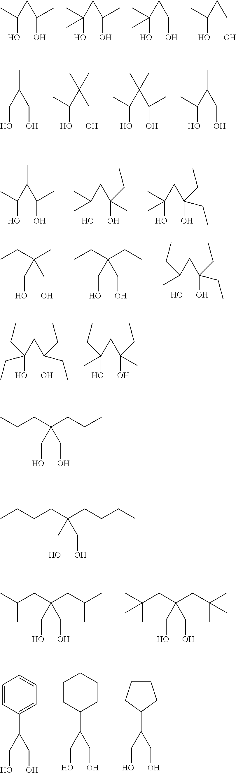
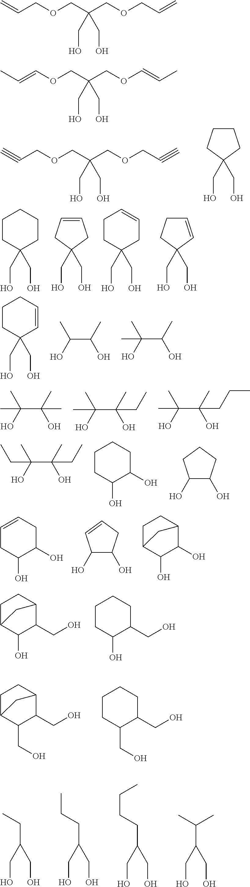
[0056]In 500 g of 2-propanol (IPA) was dissolved 284 g of titanium tetraisopropoxide. With stirring, a mixture of 27 g of deionized water and 500 g of IPA was added dropwise to the solution at room temperature over 2 hours. To the solution, 146 g of 2-ethyl-1,3-hexanediol was added, followed by stirring at room temperature for 30 minutes. The solution was concentrated in vacuum at 30° C. The concentrate was further heated to 60° C. and held at the temperature in vacuum until any distillate no longer came out. At the end of distillation, 1,200 g of 4-methyl-2-pentanol (MIBC) was added to the residue, which was heated at 40° C. in vacuum until IPA was no longer distilled out. There was obtained 1,000 g of a MIBC solution of titanium-containing compound (A-I). The compound (A-I) had a Mw of 1,000.
synthesis example a-ii
[0057]In 500 g of IPA was dissolved 284 g of titanium tetraisopropoxide. With stirring, a mixture of 27 g of deionized water and 500 g of IPA was added dropwise to the solution at room temperature over 2 hours. To the solution, 120 g of 2-methyl-2,4-pentanediol was added, followed by stirring at room temperature for 30 minutes. The solution was concentrated in vacuum at 30° C. The concentrate was further heated to 60° C. and held at the temperature in vacuum until any distillate no longer came out. At the end of distillation, 1,200 g of MIBC was added to the residue, which was heated at 40° C. in vacuum until IPA was no longer distilled out. There was obtained 1,000 g of a MIBC solution of titanium-containing compound (A-II). The compound (A-II) had a Mw of 1,100.
PUM
| Property | Measurement | Unit |
|---|---|---|
| wavelength | aaaaa | aaaaa |
| thickness | aaaaa | aaaaa |
| thickness | aaaaa | aaaaa |
Abstract
Description
Claims
Application Information