
Etching terminal checking device and method for plasma etching equipment
A technology of etching equipment and end point detection, applied in semiconductor/solid-state device testing/measurement, electrical components, semiconductor/solid-state device manufacturing, etc., can solve the difficulties of software integration and development, CCD stability, signal noise and insufficient sensitivity , high cost of testing equipment, etc., to achieve the effect of ensuring the quality of silicon wafer processing, ensuring the normal silicon wafer processing process, and improving production efficiency
Patent Information
- Authority / Receiving Office
- CN · China
- Patent Type
- Patents(China)
- Current Assignee / Owner
- Publication Date
- 2009-12-09
Smart Images
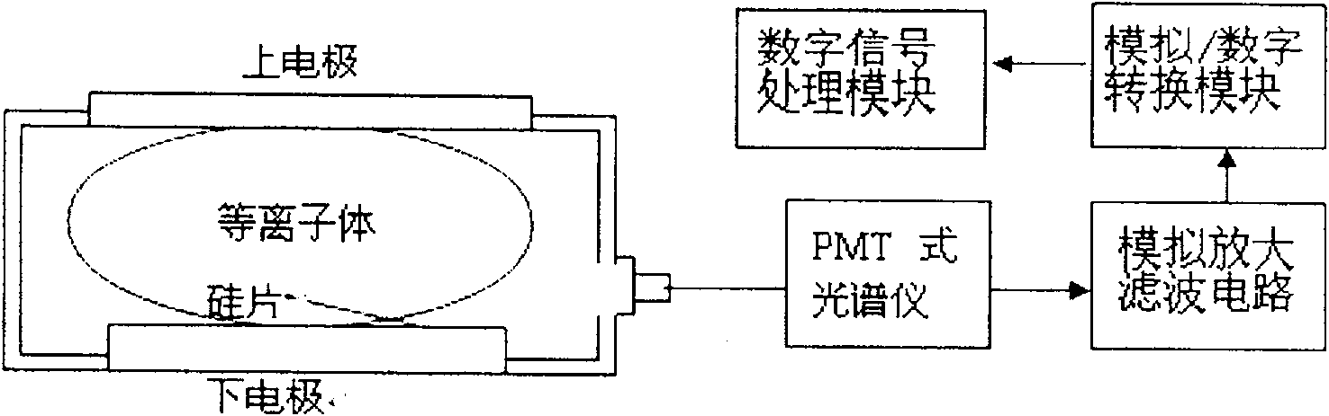
Figure 1 
Figure 2 
Figure 3
Abstract
Description
technical field
[0001] The invention relates to the technical field of microelectronic etching, in particular to an etching endpoint detection device and method for plasma etching equipment. Background technique
[0002] With the development of microelectronics technology, semiconductor chip processing technology is becoming more and more stringent, the technology node has been from 180nm to 65nm, even below 45nm, and the size of silicon wafers has also increased from 200mm to 300mm. Therefore, the process requirements for silicon wafers are becoming more and more stringent. . The etching process is one of the most complex processes in semiconductor processing. The state of the plasma and various process parameters during the etching process are directly related to the etching result.
[0003] In the structure of the plasma etching machine, the same process of etching the same type of silicon wafer should have the same etching rate and the same etching time. However, in th...
Examples
Embodiment Construction
[0030] The etching terminal detection device of a plasma etching equipment according to the present invention, its specific implementation method is as follows figure 1 As shown, it includes a spectrometer, an analog amplification and filtering circuit, an analog / digital conversion module and a digital signal processing module, wherein,
[0031] The spectrometer converts the detected optical signal inside the plasma etching equipment into an analog electrical signal output; the spectrometer is a photomultiplier tube PMT spectrometer, and the PMT receives the spectrum emitted by the plasma in the plasma etching equipment and converts the light The signal is converted into an analog electrical signal. Specifically, during the etching process, the spectrum emitted by the plasma in the reaction chamber of the plasma etching equipment is received by the photomultiplier tube of the PMT spectrometer, and the light intensity change of the spectral signal in the reaction chamber is con...