
Semiconductor element and its producing method
A manufacturing method and semiconductor technology, applied in semiconductor/solid-state device manufacturing, semiconductor devices, electrical components, etc., can solve the problems of embedded MIM capacitor limitation, chip area reduction, and inability to provide capacitance value, etc.
Patent Information
- Authority / Receiving Office
- CN · China
- Patent Type
- Applications(China)
- Current Assignee / Owner
- Publication Date
- 2007-07-25
Smart Images
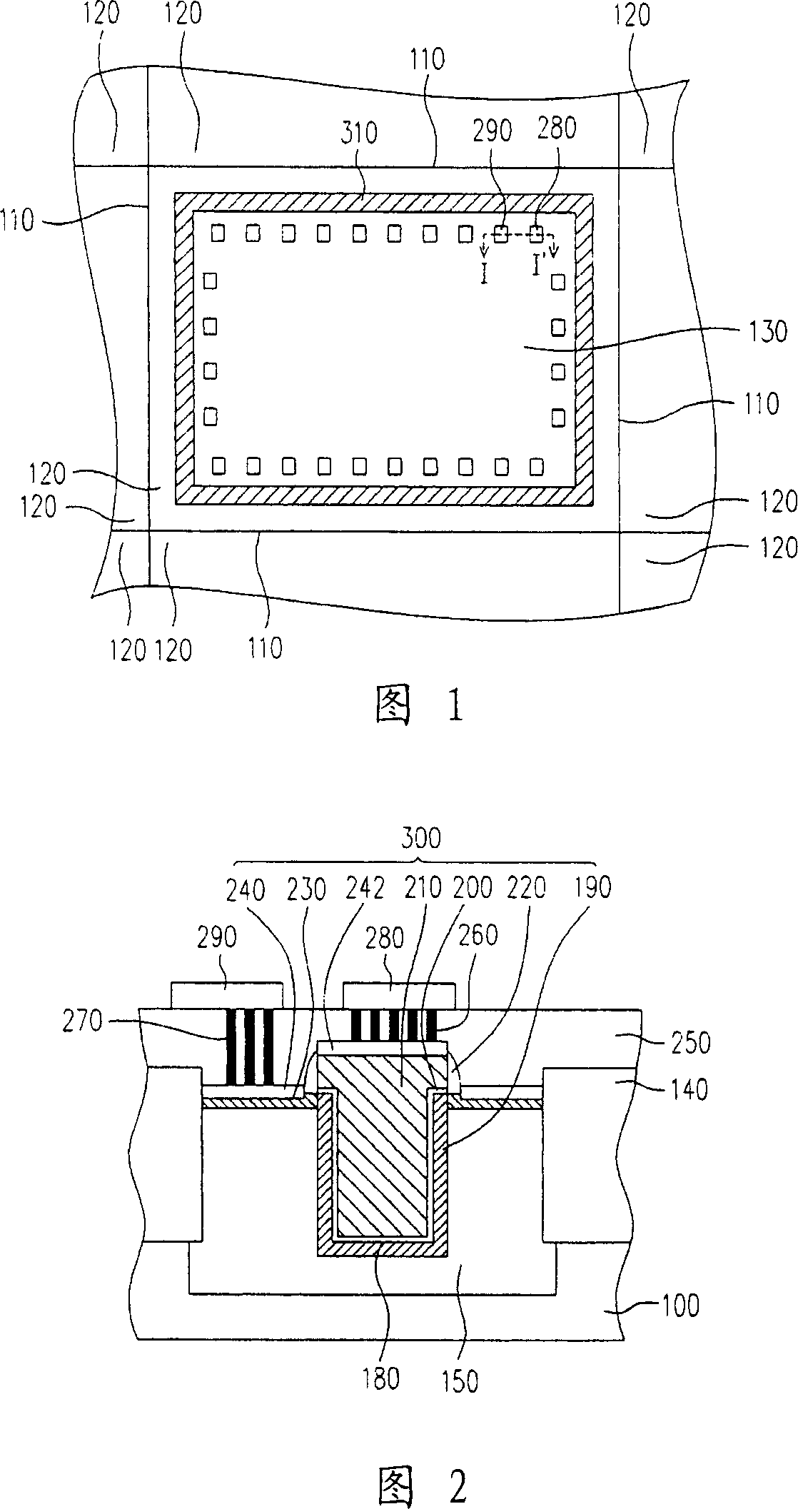
Figure 1 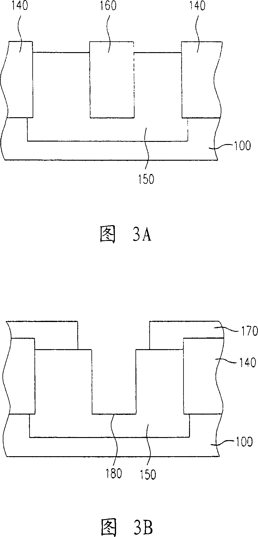
Figure 2 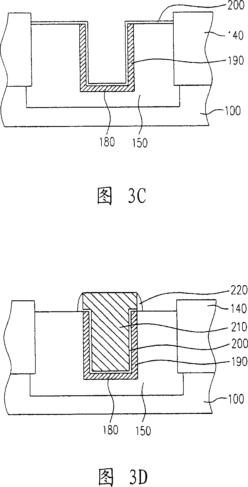
Figure 3
Abstract
Description
technical field
[0001] The invention relates to a semiconductor element and a manufacturing method thereof, in particular to a high-voltage semiconductor capacitor and a manufacturing method thereof. Background technique
[0002] With the advancement of integrated circuit manufacturing, the size of components has been continuously reduced, and metal oxide semiconductor (MOS) has become the main component of circuit design. However, since the operating voltage of the MOS transistor is getting smaller and smaller, it is easy to be damaged due to the intrusion of external noise. Industry and academia have devoted a lot of effort to the prevention of noise, and many solutions have been obtained.
[0003] When the input voltage is applied to the high-voltage components through the input pad (Input Pad), there will be similar noise problems. In order to stabilize the input voltage of the high-voltage component, a capacitor with a large capacitance (Capacitance) is arranged on th...
Examples
Embodiment Construction
[0048] Fig. 1 is a top view of a semiconductor element of a preferred embodiment of the present invention. Referring to FIG. 1 , the semiconductor device of the present invention is composed of a substrate 100 , a plurality of pads and a trench capacitor 300 . There are a plurality of dicing lines 110 on the substrate 100 , and the dicing lines 110 divide the substrate 100 into a plurality of chips 120 . That is, the area divided by the dicing line 110 is the chip area to be diced in the future. A peripheral area of the chip 120 has a plurality of bonding pads, including a bonding pad 280 and a bonding pad 290 . The trench capacitor 300 shown in FIG. 2 is disposed under the pad, or in the area 310 between the pad and the cutting line 110 . In this embodiment, the trench capacitor 300 located under the pads 280 and 290 is taken as an example for illustration.
[0049]Please continue to refer to Fig. 2, which is a cross-sectional view along the section line I-I' in Fig. 1 ....