

Inverse epitaxial wafer preparation method
A technology of epitaxial wafers and epitaxial layers, applied in semiconductor/solid-state device manufacturing, gaseous chemical plating, coating, etc., can solve the problem of small expansion resistance surface at PN junction
Patent Information
- Authority / Receiving Office
- CN · China
- Patent Type
- Patents(China)
- Current Assignee / Owner
- Publication Date
- 2011-11-30
Smart Images
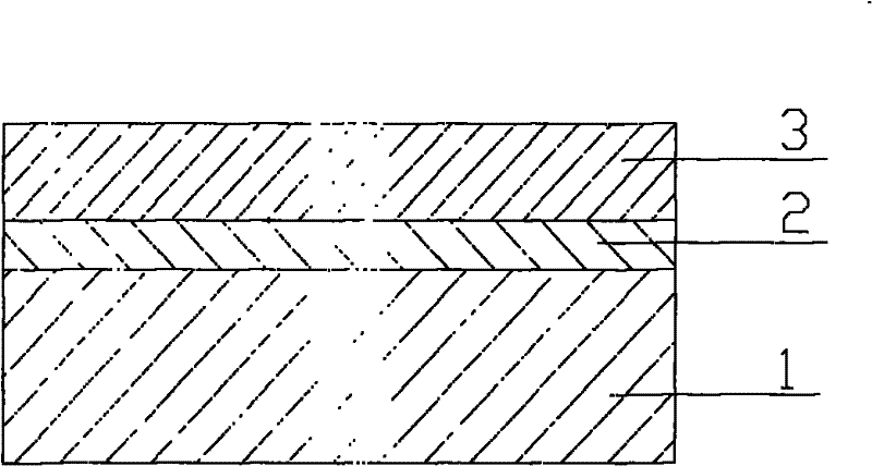
Figure 1 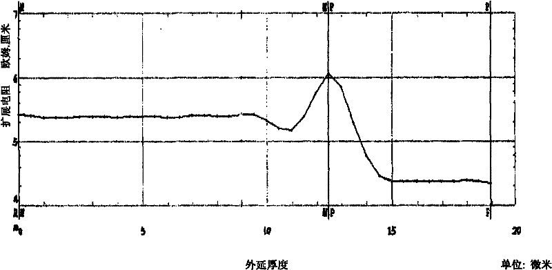
Figure 2 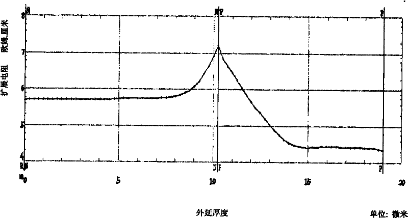
Figure 3
Abstract
Description
technical field
[0001] The invention relates to a method for preparing an epitaxial wafer, in particular to a method for preparing an inverse epitaxial wafer for preparing an N-type epitaxial layer on a P-type substrate. Background technique
[0002] The reverse epitaxial wafer refers to the epitaxial wafer in which the N-type epitaxial layer is prepared on the P-type substrate. At present, the preparation process used in production is: when the furnace temperature reaches 800-950°C, place the silicon wafer in the furnace with a manipulator, and pass through the hydrogen gas. ~1150℃, after baking, pass through hydrogen chloride for gas phase polishing; close hydrogen chloride, pass through trichlorosilane to produce intrinsic barrier layer; close trichlorosilane, use hydrogen to remove impurity gas in the furnace, and then pass through three Chlorosilane and PH 3 , grow the epitaxial layer, and finally lower the temperature to 800-950°C and take out the silicon wafer with ...
Examples
Embodiment 1
[0019] 1) Pass hydrogen through the monolithic furnace, place the P-type substrate silicon wafer into the monolithic furnace with a manipulator at 800-950°C, raise the temperature to 1140°C, and the hydrogen flow rate is 20L / min;
[0020] 2) Baking to remove the oxide layer, the time is 1min, the hydrogen flow rate is 20L / min;
[0021] 3) Conduct chemical vapor phase polishing with hydrogen chloride for 1 minute, the flow rate of hydrogen chloride is 0.3L / min, and the flow rate of hydrogen gas is 20L / min;
[0022] 4) Raise the temperature of the single-chip furnace to 1170°C, and increase the hydrogen flow rate to 100L / min;
[0023] 5) The intrinsic barrier layer is grown by trichlorosilane, the trichlorosilane flow rate: 3L / min, and the growth time is 10 seconds; the intrinsic barrier layer produced is single crystal intrinsic silicon;
[0024] 6) Turn off the trichlorosilane, keep the temperature within the range of 1170°C, and expel the gas for 50 seconds at a hydrogen flo...
Embodiment 2
[0029] 1) Pass hydrogen through the single-chip furnace, place the P-type substrate silicon wafer into the single-chip furnace with a robot at 950°C, raise the temperature to 1150°C, and the hydrogen flow rate is 80L / min;
[0030] 2) Baking to remove the oxide layer, the time is 3min, the hydrogen flow rate is 80L / min;
[0031] 3) Conduct chemical vapor phase polishing with hydrogen chloride for 1 minute, hydrogen chloride flow rate 1L / min, hydrogen flow rate 80L / min;
[0032] 4) Raise the temperature of the single-chip furnace to 1210°C, and increase the hydrogen flow rate to 200L / min;
[0033] 5) The intrinsic barrier layer is grown by trichlorosilane, the trichlorosilane flow rate: 8L / min, and the growth time is 60 seconds; the intrinsic barrier layer produced is single crystal intrinsic silicon;
[0034] 6) Turn off the trichlorosilane, keep the temperature within the range of 1210°C, and catch the gas for 120 seconds at a hydrogen flow rate of 200L / min;
[0035] 7) Redu...
Embodiment 3
[0039] 1) Pass hydrogen through the single-chip furnace, place the P-type substrate silicon wafer into the single-chip furnace with a robot at 900°C, raise the temperature to 1145°C, and the hydrogen flow rate is 60L / min;
[0040] 2) Baking to remove the oxide layer, the time is 2min, the hydrogen flow rate is 60L / min;
[0041] 3) Perform chemical vapor phase polishing with hydrogen chloride for 1 minute, the flow rate of hydrogen chloride is 0.7L / min, and the flow rate of hydrogen gas is 60L / min;
[0042] 4) Raise the temperature of the single-chip furnace to 1200°C, and increase the hydrogen flow rate to 150L / min;
[0043] 5) The intrinsic barrier layer is grown by trichlorosilane, the flow rate of trichlorosilane is 6L / min, and the growth time is 40 seconds; the intrinsic barrier layer produced is single crystal intrinsic silicon;
[0044] 6) Turn off the trichlorosilane, keep the temperature within the range of 1200°C, and expel the gas for 80 seconds at a hydrogen flow r...