
Substrate for holding at least one component and method for producing same
A technology for substrates and components, applied in semiconductor/solid-state device manufacturing, electrical components, electrical solid-state devices, etc., can solve problems such as DCB substrate fracture, and achieve the effect of simple cost
Patent Information
- Authority / Receiving Office
- CN · China
- Patent Type
- Applications(China)
- Current Assignee / Owner
- Publication Date
- 2010-08-18
- Estimated Expiration
- Not applicable · inactive patent
Smart Images
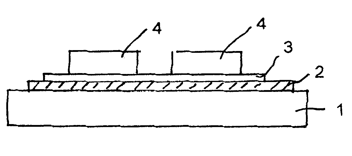
Figure 1 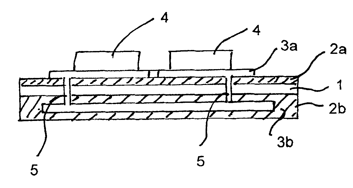
Figure 2 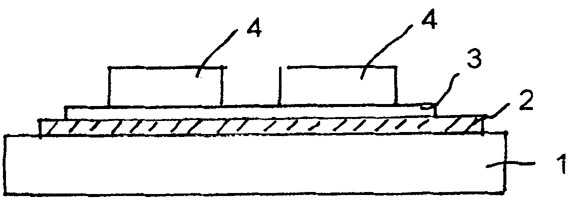
Figure 3
Abstract
Description
technical field
[0001] The invention relates to a substrate according to the preamble of claim 1 . The invention also relates to a method of manufacturing a substrate. Background technique
[0002] Substrates for receiving electrical or electronic components are generally known from the prior art. Such a substrate generally consists of a plate of electrically insulating material which is provided with an electrically conductive layer at least on the front side and / or on the opposite rear side. The plate can be made of electrically insulating plastic or ceramic, for example. In particular for the production of modules equipped with power semiconductors, direct copper-on-copper (DCB) substrates are used according to the prior art, for example. Here, plates made of aluminum oxide or aluminum nitride are used as electrical insulators. As a result, the conductor lines are applied from pure copper in a high-temperature melting and diffusion process. Such DCB substrates are di...
Examples
Embodiment Construction
[0027] exist figure 1 In this case, a connection layer 2 is provided on the substrate body 1 . The connection layer 2 connects the conductive layer 3 with the substrate body 1 . The conductive layer 3 is connected to the element 4, and the conductive layer 3 may be a conductor line structure. The component 4 can be a semiconductor component, in particular a power semiconductor. The element 4 is connected to the conductive layer 3 , for example by means of a conventional solder connection.
[0028] The connection layer 2 is electrically insulating, preferably made of polysiloxane, which is filled with fillers up to a filling degree of 60% by volume to 80% by volume. The filler is suitably SiC having an average particle size in the range of 2 to 10 μm. Such a connection layer 2 has an excellent thermal conductivity λ of greater than 20 W / mK.
[0029] The substrate body 1 is made of metal, preferably a copper alloy or an aluminum alloy. The substrate body 1 can be produced ...