
High isolation slot line duplexer applied to ultra-wideband channel and narrow-band channel
An ultra-broadband, high isolation technology, applied in waveguide-type devices, electrical components, circuits, etc., can solve the problems of increasing circuit size, unfavorable miniaturization, and difficult bandwidth adjustment, and achieve improved isolation, easy processing, and high isolation. degree of effect
Patent Information
- Authority / Receiving Office
- CN · China
- Current Assignee / Owner
- Publication Date
- 2014-05-21
- Estimated Expiration
- Not applicable · inactive patent
Smart Images
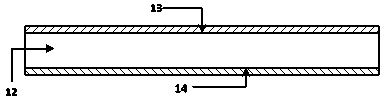
Figure 1 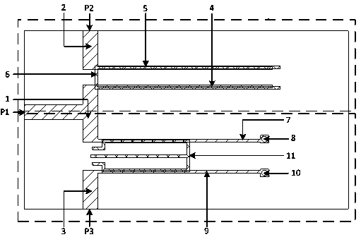
Figure 2 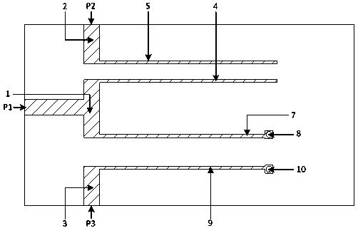
Figure 3
Abstract
Description
technical field
[0001] The invention relates to the field of duplexers, in particular to a high-isolation slotline duplexer applied to ultra-wideband channels and narrowband channels. Background technique
[0002] Microwave duplexer is an important microwave device widely used in radio receivers. It is a crucial component for modern multi-frequency multi-service transceiver systems to share the same antenna. Its performance directly affects the work of RF front-end performance. The traditional duplexer design is to design two filters separately, and then connect them through a matching network. The existence of the matching network increases the circuit size, which is not conducive to miniaturization. Accordingly, some scholars use the shared resonator technology to replace the matching network. Although this greatly reduces the circuit size, this technology can only be applied to narrow-band systems, and the bandwidth is not easy to adjust. It is necessary to design a...
Examples
Embodiment Construction
[0022] The present invention will be further described below in conjunction with accompanying drawing.
[0023] The present invention uses a PCB board with a relative dielectric constant of 2.2 and a thickness of 0.508mm as the substrate, and a PCB board of other specifications may also be used as the substrate. Such as figure 1 As shown, the upper and lower surfaces of the dielectric substrate 12 of the PCB are respectively coated with an upper metal patch 13 and a lower metal patch 14 . The upper layer microstrip line structure described below is formed on the upper layer of the dielectric substrate, and the slot line structure is formed after the lower metal patch 14 is etched.
[0024] figure 2 It is a structural schematic diagram of a slotted line duplexer. In the figure, the U-shaped slotted line resonator 6 and the multimode slotted line resonator 11 are located on the lower layer of the dielectric substrate, and the rest of the microstrip line structures are located...